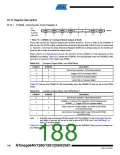
20.6.1
Compare Output Mode and Waveform Generation
The Waveform Generator uses the COM2x1:0 bits differently in normal, CTC, and PWM modes.
For all modes, setting the COM2x1:0 = 0 tells the Waveform Generator that no action on the
OC2x Register is to be performed on the next compare match. For compare output actions in the
non-PWM modes refer to Table 20-5 on page 189. For fast PWM mode, refer to Table 20-6 on
page 189, and for phase correct PWM refer to Table 20-7 on page 190.
A change of the COM2x1:0 bits state will have effect at the first compare match after the bits are
written. For non-PWM modes, the action can be forced to have immediate effect by using the
FOC2x strobe bits.
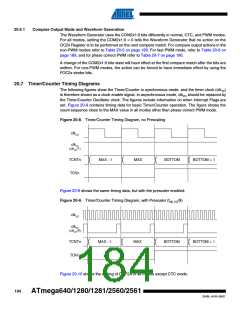
20.7 Timer/Counter Timing Diagrams
The following figures show the Timer/Counter in synchronous mode, and the timer clock (clkT2)
is therefore shown as a clock enable signal. In asynchronous mode, clkI/O should be replaced by
the Timer/Counter Oscillator clock. The figures include information on when Interrupt Flags are
set. Figure 20-8 contains timing data for basic Timer/Counter operation. The figure shows the
count sequence close to the MAX value in all modes other than phase correct PWM mode.
Figure 20-8. Timer/Counter Timing Diagram, no Prescaling
clkI/O
clkTn
(clkI/O/1)
TCNTn
TOVn
MAX - 1
MAX
BOTTOM
BOTTOM + 1
Figure 20-9 shows the same timing data, but with the prescaler enabled.
Figure 20-9. Timer/Counter Timing Diagram, with Prescaler (fclk_I/O/8)
clkI/O
clkTn
(clkI/O/8)
TCNTn
TOVn
MAX - 1
MAX
BOTTOM
BOTTOM + 1
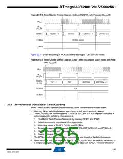
Figure 20-10 shows the setting of OCF2A in all modes except CTC mode.
184
ATmega640/1280/1281/2560/2561
2549L–AVR–08/07

 ATMEL [ ATMEL ]