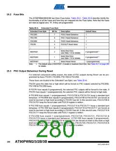
AT90PWM2/3/2B/3B
Table 25-5. Fuse High Byte
High Fuse Byte
RSTDISBL(1)
DWEN
Bit No
Description
Default Value
7
6
External Reset Disable
debugWIRE Enable
1 (unprogrammed)
1 (unprogrammed)
Enable Serial Program and
Data Downloading
0 (programmed, SPI
programming enabled)
SPIEN(2)
5
4
WDTON(3)
Watchdog Timer Always On
1 (unprogrammed)
EEPROM memory is
preserved through the Chip
Erase
1 (unprogrammed), EEPROM
not reserved
EESAVE
3
Brown-out Detector trigger
level
BODLEVEL2(4)
BODLEVEL1(4)
BODLEVEL0(4)
2
1
0
1 (unprogrammed)
1 (unprogrammed)
1 (unprogrammed)
Brown-out Detector trigger
level
Brown-out Detector trigger
level
Notes: 1. See “Alternate Functions of Port C” on page 70 for description of RSTDISBL Fuse.
2. The SPIEN Fuse is not accessible in serial programming mode.
3. See “Watchdog Timer Configuration” on page 54 for details.
4. See Table 9-2 on page 48 for BODLEVEL Fuse decoding.
Table 25-6. Fuse Low Byte
Low Fuse Byte
CKDIV8(4)
CKOUT(3)
SUT1
Bit No
Description
Default Value
7
6
5
4
3
2
1
0
Divide clock by 8
Clock output
0 (programmed)
1 (unprogrammed)
1 (unprogrammed)(1)
0 (programmed)(1)
0 (programmed)(2)
0 (programmed)(2)
1 (unprogrammed)(2)
0 (programmed)(2)
Select start-up time
Select start-up time
Select Clock source
Select Clock source
Select Clock source
Select Clock source
SUT0
CKSEL3
CKSEL2
CKSEL1
CKSEL0
Note:
1. The default value of SUT1..0 results in maximum start-up time for the default clock source.
See Table 7-11 on page 37 for details.
2. The default setting of CKSEL3..0 results in internal RC Oscillator @ 8 MHz. See Table 7-11 on
page 37 for details.
3. The CKOUT Fuse allows the system clock to be output on PORTB0. See “Clock Output Buffer”
on page 37 for details.
4. See “System Clock Prescaler” on page 37 for details.
The status of the Fuse bits is not affected by Chip Erase. Note that the Fuse bits are locked if
Lock bit1 (LB1) is programmed. Program the Fuse bits before programming the Lock bits.
25.3.1
Latching of Fuses
The fuse values are latched when the device enters programming mode and changes of the
fuse values will have no effect until the part leaves Programming mode. This does not apply to
the EESAVE Fuse which will take effect once it is programmed. The fuses are also latched on
Power-up in Normal mode.
281
4317J–AVR–08/10

 ATMEL [ ATMEL ]