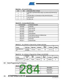
Table 25-9. XA1 and XA0 Coding
XA1
XA0
Action when XTAL1 is Pulsed
Load Flash or EEPROM Address (High or low address byte determined by
BS1).
0
0
0
1
1
1
0
1
Load Data (High or Low data byte for Flash determined by BS1).
Load Command
No Action, Idle
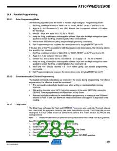
Table 25-10. Command Byte Bit Coding
Command Byte
1000 0000
0100 0000
0010 0000
0001 0000
0001 0001
0000 1000
0000 0100
0000 0010
0000 0011
Command Executed
Chip Erase
Write Fuse bits
Write Lock bits
Write Flash
Write EEPROM
Read Signature Bytes and Calibration byte
Read Fuse and Lock bits
Read Flash
Read EEPROM
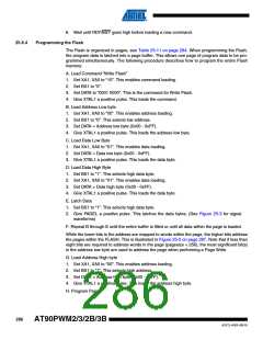
Table 25-11. No. of Words in a Page and No. of Pages in the Flash
No. of
Device
Flash Size
Page Size
PCWORD
Pages
PCPAGE
PCMSB
AT90PWM2/2B/3/
3B
4K words
(8K bytes)
32 words
PC[4:0]
128
PC[11:5]
11
Table 25-12. No. of Words in a Page and No. of Pages in the EEPROM
EEPROM
Size
Page
Size
No. of
Pages
Device
PCWORD
PCPAGE
EEAMSB
AT90PWM2/2B/3/
3B
512 bytes
4 bytes
EEA[1:0]
128
EEA[8:2]
8
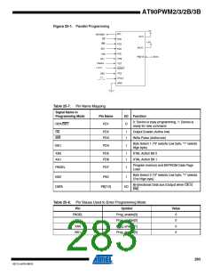
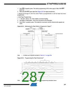
25.7 Serial Programming Pin Mapping
Table 25-13. Pin Mapping Serial Programming
Symbol
MOSI_A
MISO_A
SCK_A
Pins
PD3
PD2
PD4
I/O
Description
Serial Data in
Serial Data out
Serial Clock
I
O
I
284
AT90PWM2/3/2B/3B
4317J–AVR–08/10

 ATMEL [ ATMEL ]