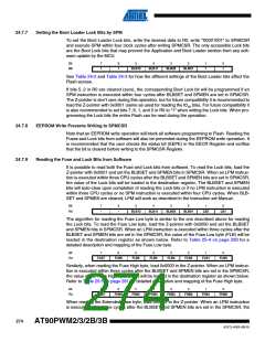
For details about these two section, see “NRWW – No Read-While-Write Section” on page 266
and “RWW – Read-While-Write Section” on page 266
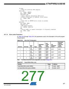
Table 24-8. Explanation of Different Variables used in Figure 24-3 and the Mapping to the Z-
pointer
Corresponding
Variable
Z-value(1)
Description
Most significant bit in the Program Counter. (The
Program Counter is 12 bits PC[11:0])
PCMSB
11
4
Most significant bit which is used to address the
words within one page (32 words in a page requires
5 bits PC [4:0]).
PAGEMSB
ZPCMSB
Bit in Z-register that is mapped to PCMSB. Because
Z0 is not used, the ZPCMSB equals PCMSB + 1.
Z12
Z5
Bit in Z-register that is mapped to PAGEMSB.
Because Z0 is not used, the ZPAGEMSB equals
PAGEMSB + 1.
ZPAGEMSB
PCPAGE
Program counter page address: Page select, for
page erase and page write
PC[11:5]
PC[4:0]
Z12:Z6
Z5:Z1
Program counter word address: Word select, for
filling temporary buffer (must be zero during page
write operation)
PCWORD
Note:
1. Z15:Z13: always ignored
Z0: should be zero for all SPM commands, byte select for the LPM instruction.
See “Addressing the Flash During Self-Programming” on page 271 for details about the use of
Z-pointer during Self-Programming.
25. Memory Programming
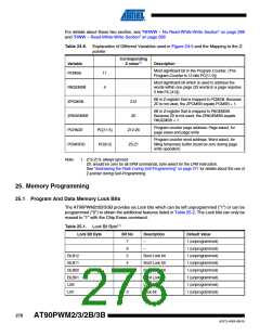
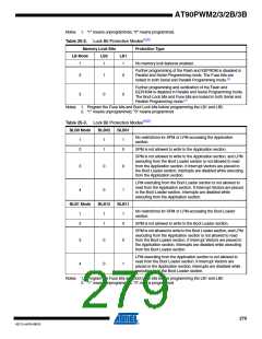
25.1 Program And Data Memory Lock Bits
The AT90PWM2/2B/3/3B provides six Lock bits which can be left unprogrammed (“1”) or can be
programmed (“0”) to obtain the additional features listed in Table 25-2. The Lock bits can only be
erased to “1” with the Chip Erase command.
Table 25-1. Lock Bit Byte(1)
Lock Bit Byte
Bit No
Description
–
Default Value
7
6
5
4
3
2
1
0
1 (unprogrammed)
1 (unprogrammed)
1 (unprogrammed)
1 (unprogrammed)
1 (unprogrammed)
1 (unprogrammed)
1 (unprogrammed)
1 (unprogrammed)
–
BLB12
Boot Lock bit
Boot Lock bit
Boot Lock bit
Boot Lock bit
Lock bit
BLB11
BLB02
BLB01
LB2
LB1
Lock bit
278
AT90PWM2/3/2B/3B
4317J–AVR–08/10

 ATMEL [ ATMEL ]