AT90PWM2/3/2B/3B
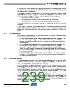
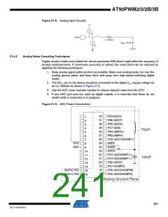
Figure 21-8. Analog Input Circuitry
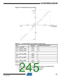
I
IH
ADCn
1..100 kΩ
C
= 14 pF
V
S/H
I
IL
/2
CC
21.6.2
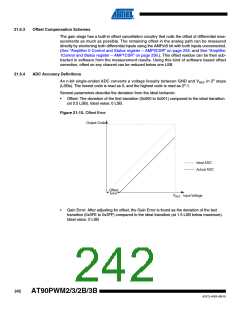
Analog Noise Canceling Techniques
Digital circuitry inside and outside the device generates EMI which might affect the accuracy of
analog measurements. If conversion accuracy is critical, the noise level can be reduced by
applying the following techniques:
1. Keep analog signal paths as short as possible. Make sure analog tracks run over the
analog ground plane, and keep them well away from high-speed switching digital
tracks.
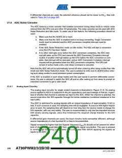
2. The AVCC pin on the device should be connected to the digital VCC supply voltage via
an LC network as shown in Figure 21-9.
3. Use the ADC noise canceler function to reduce induced noise from the CPU.
4. If any ADC port pins are used as digital outputs, it is essential that these do not
switch while a conversion is in progress.
Figure 21-9. ADC Power Connections
32
31
30
29
28
27
26
25
24
23
22
21
20
19
18
17
PB7(ADC4)
1
PB6 (ADC7)
2
PB5 (ADC6)
3
PC7 (D2A)
4
10μH
PB4 (AMP0+)
PB3 (AMP0-)
PC6 (ADC10/ACMP1)
AREF
5
6
7
VCC
GND
8
AGND
9
AVCC
10
11
12
13
14
15
16
PC5 (ADC9/AMP1+)
PC4 (ADC8/AMP1-)
PB2 (ADC5)
100nF
PD7 (ACMP0)
PD6 (ADC3/ACMPM)
PD5 (ADC2/ACMP2)
(ADC0) PE2
(ADC1) PD4
Analog Ground Plane
241
4317J–AVR–08/10

 ATMEL [ ATMEL ]