global interrupts are enabled). UDRE is cleared by writing UDR. When interrupt-driven data
transmission is used, the Data Register Empty interrupt routine must either write new data to
UDR in order to clear UDRE or disable the Data Register Empty interrupt, otherwise a new inter-
rupt will occur once the interrupt routine terminates.
The Transmit Complete (TXC) flag bit is set one when the entire frame in the Transmit Shift Reg-
ister has been shifted out and there are no new data currently present in the transmit buffer. The
TXC flag bit is automatically cleared when a transmit complete interrupt is executed, or it can be
cleared by writing a one to its bit location. The TXC flag is useful in half-duplex communication
interfaces (like the RS-485 standard), where a transmitting application must enter receive mode
and free the communication bus immediately after completing the transmission.
When the Transmit Complete Interrupt Enable (TXCIE) bit in UCSRB is set, the USART Trans-
mit Complete Interrupt will be executed when the TXC flag becomes set (provided that global
interrupts are enabled). When the transmit complete interrupt is used, the interrupt handling rou-
tine does not have to clear the TXC flag, this is done automatically when the interrupt is
executed.
18.6.4
18.6.5
Parity Generator
The Parity Generator calculates the parity bit for the serial frame data. When parity bit is enabled
(UPM1 = 1), the transmitter control logic inserts the parity bit between the last data bit and the
first stop bit of the frame that is sent.
Disabling the Transmitter
The disabling of the Transmitter (setting the TXEN to zero) will not become effective until ongo-
ing and pending transmissions are completed, i.e., when the Transmit Shift Register and
Transmit Buffer Register do not contain data to be transmitted. When disabled, the Transmitter
will no longer override the TxD pin.
18.7 Data Reception – USART Receiver
The USART Receiver is enabled by writing the Receive Enable (RXEN) bit in the UCSRB Regis-
ter to one. When the Receiver is enabled, the normal pin operation of the RxD pin is overridden
by the USART and given the function as the Receiver’s serial input. The baud rate, mode of
operation and frame format must be set up once before any serial reception can be done. If syn-
chronous operation is used, the clock on the XCK pin will be used as transfer clock.
18.7.1
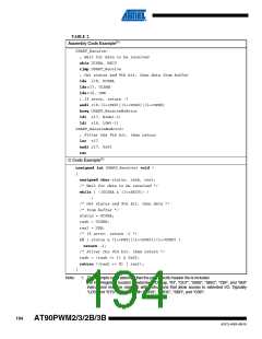
Receiving Frames with 5 to 8 Data Bits
The Receiver starts data reception when it detects a valid start bit. Each bit that follows the start
bit will be sampled at the baud rate or XCK clock, and shifted into the Receive Shift Register until
the first stop bit of a frame is received. A second stop bit will be ignored by the Receiver. When
the first stop bit is received, i.e., a complete serial frame is present in the Receive Shift Register,
the contents of the Shift Register will be moved into the receive buffer. The receive buffer can
then be read by reading the UDR I/O location.
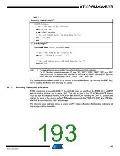
The following code example shows a simple USART receive function based on polling of the
Receive Complete (RXC) flag. When using frames with less than eight bits the most significant
bits of the data read from the UDR will be masked to zero. The USART has to be initialized
before the function can be used.
192
AT90PWM2/3/2B/3B
4317J–AVR–08/10

 ATMEL [ ATMEL ]