Figure 18-5. Data OverRun example
RxD
CH1
CH2
CH3
DOR
RxC
t
RxC=1
UDR=CH2
DOR=0
RxC=1
UDR=XX
DOR=1
RxC=1
UDR=CH1
DOR=0
Software Access
to Receive buffer
The Parity Error (UPE) Flag indicates that the next frame in the receive buffer had a Parity Error
when received. If Parity Check is not enabled the UPE bit will always be read zero. For compati-
bility with future devices, always set this bit to zero when writing to UCSRA. For more details see
“Parity Bit Calculation” on page 188 and “Parity Checker” on page 196.
18.7.5
Parity Checker
The Parity Checker is active when the high USART Parity mode (UPM1) bit is set. Type of Parity
Check to be performed (odd or even) is selected by the UPM0 bit. When enabled, the Parity
Checker calculates the parity of the data bits in incoming frames and compares the result with
the parity bit from the serial frame. The result of the check is stored in the receive buffer together
with the received data and stop bits. The Parity Error (UPE) flag can then be read by software to
check if the frame had a Parity Error.
The UPE bit is set if the next character that can be read from the receive buffer had a Parity
Error when received and the Parity Checking was enabled at that point (UPM1 = 1). This bit is
valid until the receive buffer (UDR) is read.
18.7.6
18.7.7
Disabling the Receiver
In contrast to the Transmitter, disabling of the Receiver will be immediate. Data from ongoing
receptions will therefore be lost. When disabled (i.e., the RXEN is set to zero) the Receiver will
no longer override the normal function of the RxD port pin. The Receiver buffer FIFO will be
flushed when the Receiver is disabled. Remaining data in the buffer will be lost
Flushing the Receive Buffer
The receiver buffer FIFO will be flushed when the Receiver is disabled, i.e., the buffer will be
emptied of its contents. Unread data will be lost. If the buffer has to be flushed during normal
operation, due to for instance an error condition, read the UDR I/O location until the RXC flag is
cleared.
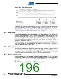
The following code example shows how to flush the receive buffer.
196
AT90PWM2/3/2B/3B
4317J–AVR–08/10

 ATMEL [ ATMEL ]