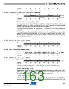
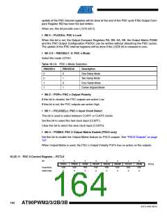
AT90PWM2/3/2B/3B
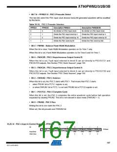
• Bit 7:6 – PPRE21:0 : PSC 2 Prescaler Select
This two bits select the PSC input clock division factor.All generated waveform will be modified
by this factor.
Table 16-16. PSC 2 Prescaler Selection
PPRE21
PPRE20
Description PWM2/3
Description PWM2B/3B
0
0
1
1
0
1
0
1
No divider on PSC input clock
Divide the PSC input clock by 4
Divide the PSC input clock by 16
Divide the PSC clock by 64
No divider on PSC input clock
Divide the PSC input clock by 4
Divide the PSC input clock by 32
Divide the PSC clock by 256
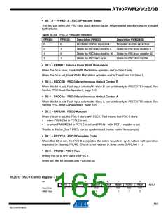
• Bit 5 – PBFM2 : Balance Flank Width Modulation
When this bit is clear, Flank Width Modulation operates on On-Time 1 only.
When this bit is set, Flank Width Modulation operates on On-Time 0 and On-Time 1.
• Bit 4 – PAOC2B : PSC 2 Asynchronous Output Control B
When this bit is set, Fault input selected to block B can act directly to PSCOUT21 and
PSCOUT23 outputs. See Section “PSC Clock Sources”, page 159.
• Bit 3 – PAOC2A : PSC 2 Asynchronous Output Control A
When this bit is set, Fault input selected to block A can act directly to PSCOUT20 and
PSCOUT22 outputs. See Section “PSC Clock Sources”, page 159.
• Bit 2 – PARUN2 : PSC 2 Autorun
When this bit is set, the PSC 2 starts with PSC1. That means that PSC 2 starts :
•
•
when PRUN1 bit in PCTL1 register is set,
or when PARUN1 bit in PCTL1 is set and PRUN0 bit in PCTL0 register is set.
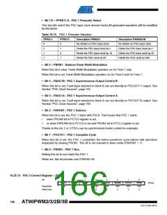
• Bit 1 – PCCYC2 : PSC 2 Complete Cycle
When this bit is set, the PSC 2 completes the entire waveform cycle before halt operation
requested by clearing PRUN2. This bit is not relevant in slave mode (PARUN2 = 1).
• Bit 0 – PRUN2 : PSC 2 Run
Writing this bit to one starts the PSC 2.
When set, this bit prevails over PARUN2 bit.
16.25.14 PSC n Input A Control Register – PFRCnA
Bit
7
6
5
4
3
2
1
0
PFRCnA
PCAEnA
PISELnA PELEVnA PFLTEnA PRFMnA3 PRFMnA2 PRFMnA1 PRFMnA0
Read/Write
Initial Value
R/W
0
R/W
0
R/W
0
R/W
0
R/W
0
R/W
0
R/W
0
R/W
0
167
4317J–AVR–08/10

 ATMEL [ ATMEL ]