AT90PWM2/3/2B/3B
16.25 PSC Register Definition
Registers are explained for PSC0. They are identical for PSC1. For PSC2 only different registers
are described.
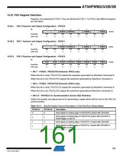
16.25.1 PSC 0 Synchro and Output Configuration – PSOC0
Bit
7
6
5
4
PSYNC00
R/W
3
-
2
POEN0B
R/W
0
1
-
0
POEN0A
R/W
0
-
-
PSYNC01
PSOC0
PSOC1
PSOC2
Read/Write
Initial Value
R/W
0
R/W
0
R/W
0
R/W
0
R/W
0
0
16.25.2 PSC 1 Synchro and Output Configuration – PSOC1
Bit
7
-
6
-
5
PSYNC11
R/W
4
PSYNC10
R/W
3
-
2
POEN1B
R/W
0
1
-
0
POEN1A
R/W
0
Read/Write
Initial Value
R/W
0
R/W
0
R/W
0
R/W
0
0
0
16.25.3 PSC 2 Synchro and Output Configuration – PSOC2
Bit
7
POS23
R/W
0
6
POS22
R/W
0
5
PSYNC21
R/W
4
PSYNC20
R/W
3
POEN2D
R/W
0
2
POEN2B
R/W
0
1
POEN2C
R/W
0
0
POEN2A
R/W
0
Read/Write
Initial Value
0
0
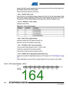
• Bit 7 – POS23 : PSCOUT23 Selection (PSC2 only)
When this bit is clear, PSCOUT23 outputs the waveform generated by Waveform Generator B.
When this bit is set, PSCOUT23 outputs the waveform generated by Waveform Generator A.
• Bit 6 – POS22 : PSCOUT22 Selection (PSC2 only)
When this bit is clear, PSCOUT22 outputs the waveform generated by Waveform Generator A.
When this bit is set, PSCOUT22 outputs the waveform generated by Waveform Generator B.
• Bit 5:4 – PSYNCn1:0: Synchronization Out for ADC Selection
Select the polarity and signal source for generating a signal which will be sent to the ADC for
synchronization.
Table 16-11. Synchronization Source Description in One/Two/Four Ramp Modes
PSYNCn1
PSYNCn0
Description
0
0
Send signal on leading edge of PSCOUTn0 (match with OCRnSA)
Send signal on trailing edge of PSCOUTn0 (match with OCRnRA or
fault/retrigger on part A)
0
1
1
1
0
1
Send signal on leading edge of PSCOUTn1 (match with OCRnSB)
Send signal on trailing edge of PSCOUTn1 (match with OCRnRB or
fault/retrigger on part B)
161
4317J–AVR–08/10

 ATMEL [ ATMEL ]