AT89S8252
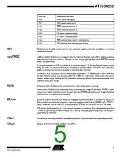
SPI Registers Control and status bits for the Serial Peripheral Interface are contained in
registers SPCR (shown in Table 4) and SPSR (shown in Table 5). The SPI data bits are
contained in the SPDR register. Writing the SPI data register during serial data transfer
sets the Write Collision bit, WCOL, in the SPSR register. The SPDR is double buffered
for writing and the values in SPDR are not changed by Reset.
Interrupt Registers The global interrupt enable bit and the individual interrupt enable
bits are in the IE register. In addition, the individual interrupt enable bit for the SPI is in
the SPCR register. Two priorities can be set for each of the six interrupt sources in the
IP register.
Dual Data Pointer Registers To facilitate accessing both internal EEPROM and exter-
nal data memory, two banks of 16-bit Data Pointer Registers are provided: DP0 at SFR
address locations 82H-83H and DP1 at 84H-85H. Bit DPS = 0 in SFR WMCON selects
DP0 and DPS = 1 selects DP1. The user should ALWAYS initialize the DPS bit to the
appropriate value before accessing the respective Data Pointer Register.
Power Off Flag The Power Off Flag (POF) is located at bit_4 (PCON.4) in the PCON
SFR. POF is set to “1” during power up. It can be set and reset under software control
and is not affected by RESET.
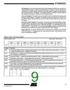
Table 4. SPCR – SPI Control Register
SPCR Address = D5H
Reset Value = 0000 01XXB
SPIE
SPE
6
DORD
5
MSTR
4
CPOL
3
CPHA
2
SPR1
1
SPR0
0
Bit
7
Symbol
Function
SPIE
SPI Interrupt Enable. This bit, in conjunction with the ES bit in the IE register, enables SPI interrupts: SPIE = 1 and ES =
1 enable SPI interrupts. SPIE = 0 disables SPI interrupts.
SPE
SPI Enable. SPI = 1 enables the SPI channel and connects SS, MOSI, MISO and SCK to pins P1.4, P1.5, P1.6, and P1.7.
SPI = 0 disables the SPI channel.
DORD
MSTR
CPOL
Data Order. DORD = 1 selects LSB first data transmission. DORD = 0 selects MSB first data transmission.
Master/Slave Select. MSTR = 1 selects Master SPI mode. MSTR = 0 selects Slave SPI mode.
Clock Polarity. When CPOL = 1, SCK is high when idle. When CPOL = 0, SCK of the master device is low when not
transmitting. Please refer to figure on SPI Clock Phase and Polarity Control.
CPHA
Clock Phase. The CPHA bit together with the CPOL bit controls the clock and data relationship between master and
slave. Please refer to figure on SPI Clock Phase and Polarity Control.
SPR0
SPR1
SPI Clock Rate Select. These two bits control the SCK rate of the device configured as master. SPR1 and SPR0 have no
effect on the slave. The relationship between SCK and the oscillator frequency, FOSC., is as follows:
SPR1 SPR0 SCK = FOSC. divided by
0
0
1
1
0
1
0
1
4
16
64
128
9
0401G–MICRO–3/06

 ATMEL [ ATMEL ]