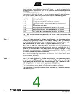
Watchdog and Memory Control Register The WMCON register contains control bits for the Watchdog Timer (shown in
Table 3). The EEMEN and EEMWE bits are used to select the 2K bytes on-chip EEPROM, and to enable byte-write. The
DPS bit selects one of two DPTR registers available.
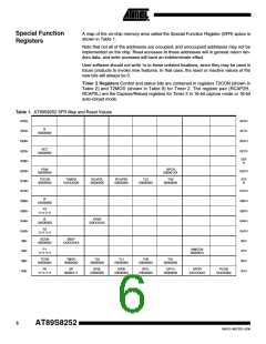
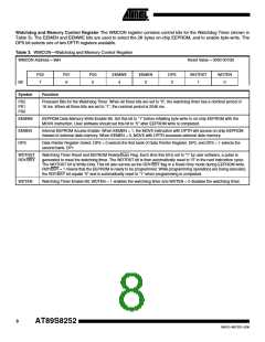
Table 3. WMCON—Watchdog and Memory Control Register
WMCON Address = 96H
Reset Value = 0000 0010B
PS2
PS1
6
PS0
5
EEMWE
4
EEMEN
3
DPS
2
WDTRST
1
WDTEN
0
Bit
7
Symbol
Function
PS2
PS1
PS0
Prescaler Bits for the Watchdog Timer. When all three bits are set to “0”, the watchdog timer has a nominal period of
16 ms. When all three bits are set to “1”, the nominal period is 2048 ms.
EEMWE
EEMEN
DPS
EEPROM Data Memory Write Enable Bit. Set this bit to “1” before initiating byte write to on-chip EEPROM with the
MOVX instruction. User software should set this bit to “0” after EEPROM write is completed.
Internal EEPROM Access Enable. When EEMEN = 1, the MOVX instruction with DPTR will access on-chip EEPROM
instead of external data memory. When EEMEN = 0, MOVX with DPTR accesses external data memory.
Data Pointer Register Select. DPS = 0 selects the first bank of Data Pointer Register, DP0, and DPS = 1 selects the
second bank, DP1
WDTRST
RDY/BSY
Watchdog Timer Reset and EEPROM Ready/Busy Flag. Each time this bit is set to “1” by user software, a pulse is
generated to reset the watchdog timer. The WDTRST bit is then automatically reset to “0” in the next instruction cycle.
The WDTRST bit is Write-Only. This bit also serves as the RDY/BSY flag in a Read-Only mode during EEPROM write.
RDY/BSY = 1 means that the EEPROM is ready to be programmed. While programming operations are being executed,
the RDY/BSY bit equals “0” and is automatically reset to “1” when programming is completed.
WDTEN
Watchdog Timer Enable Bit. WDTEN = 1 enables the watchdog timer and WDTEN = 0 disables the watchdog timer.
8
AT89S8252
0401G–MICRO–3/06

 ATMEL [ ATMEL ]