AT90USB64/128
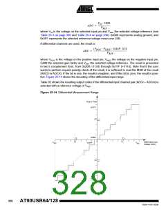
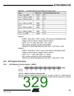
Table 25-2. Correlation Between Input Voltage and Output Codes
VADCn
Read code
0x1FF
0x1FF
0x1FE
...
Corresponding decimal value
VADCm + VREF /GAIN
VADCm + 0.999 VREF /GAIN
511
511
510
...
VADCm + 0.998 VREF /GAIN
...
VADCm + 0.001 VREF /GAIN
0x001
0x000
0x3FF
...
1
VADCm
0
VADCm - 0.001 VREF /GAIN
...
-1
...
V
ADCm - 0.999 VREF /GAIN
0x201
0x200
-511
-512
VADCm - VREF /GAIN
Example 1:
– ADMUX = 0xED (ADC3 - ADC2, 10x gain, 2.56V reference, left adjusted result)
– Voltage on ADC3 is 300 mV, voltage on ADC2 is 500 mV.
– ADCR = 512 * 10 * (300 - 500) / 2560 = -400 = 0x270
– ADCL will thus read 0x00, and ADCH will read 0x9C.
Writing zero to ADLAR right adjusts the result: ADCL = 0x70, ADCH = 0x02.
Example 2:
– ADMUX = 0xFB (ADC3 - ADC2, 1x gain, 2.56V reference, left adjusted result)
– Voltage on ADC3 is 300 mV, voltage on ADC2 is 500 mV.
– ADCR = 512 * 1 * (300 - 500) / 2560 = -41 = 0x029.
– ADCL will thus read 0x40, and ADCH will read 0x0A.
Writing zero to ADLAR right adjusts the result: ADCL = 0x00, ADCH = 0x29.
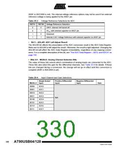
25.8 ADC Register Description
25.8.1
ADC Multiplexer Selection Register – ADMUX
Bit
7
REFS1
R/W
0
6
REFS0
R/W
0
5
ADLAR
R/W
0
4
MUX4
R/W
0
3
MUX3
R/W
0
2
MUX2
R/W
0
1
MUX1
R/W
0
0
MUX0
R/W
0
ADMUX
Read/Write
Initial Value
• Bit 7:6 – REFS1:0: Reference Selection Bits
These bits select the voltage reference for the ADC, as shown in Table 25-3. If these bits are
changed during a conversion, the change will not go in effect until this conversion is complete
329
7593A–AVR–02/06

 ATMEL [ ATMEL ]