(ADIF in ADCSRA is set). The internal voltage reference options may not be used if an external
reference voltage is being applied to the AREF pin.
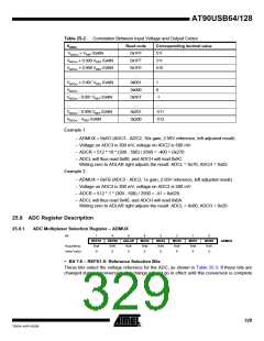
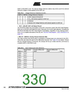
Table 25-3. Voltage Reference Selections for ADC
REFS1
REFS0 Voltage Reference Selection
0
0
1
1
0
1
0
1
AREF, Internal Vref turned off
AVCC with external capacitor on AREF pin
Reserved
Internal 2.56V Voltage Reference with external capacitor on AREF pin
•
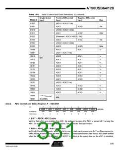
Bit 5 – ADLAR: ADC Left Adjust Result
The ADLAR bit affects the presentation of the ADC conversion result in the ADC Data Register.
Write one to ADLAR to left adjust the result. Otherwise, the result is right adjusted. Changing the
ADLAR bit will affect the ADC Data Register immediately, regardless of any ongoing conver-
sions. For a complete description of this bit, see “The ADC Data Register – ADCL and ADCH” on
page 332.
• Bits 4:0 – MUX4:0: Analog Channel Selection Bits
The value of these bits selects which combination of analog inputs are connected to the ADC.
These bits also select the gain for the differential channels. See Table 25-4 for details. If these
bits are changed during a conversion, the change will not go in effect until this conversion is
complete (ADIF in ADCSRA is set).
Table 25-4. Input Channel and Gain Selections
Single Ended
MUX4..0 Input
Positive Differential
Input
Negative Differential
Input
Gain
00000
00001
00010
00011
00100
00101
00110
00111
ADC0
ADC1
ADC2
ADC3
ADC4
ADC5
ADC6
ADC7
N/A
330
AT90USB64/128
7593A–AVR–02/06

 ATMEL [ ATMEL ]