AT90USB64/128
25.6.2
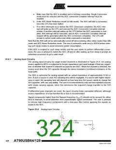
Analog Noise Canceling Techniques
Digital circuitry inside and outside the device generates EMI which might affect the accuracy of
analog measurements. If conversion accuracy is critical, the noise level can be reduced by
applying the following techniques:
a. Keep analog signal paths as short as possible. Make sure analog tracks run over
the analog ground plane, and keep them well away from high-speed switching digi-
tal tracks.
b. The AVCC pin on the device should be connected to the digital VCC supply voltage
via an LC network as shown in Figure 25-9.
c. Use the ADC noise canceler function to reduce induced noise from the CPU.
d. If any ADC port pins are used as digital outputs, it is essential that these do not
switch while a conversion is in progress.
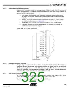
Figure 25-9. ADC Power Connections
(AD0) PA0 51
VCC
52
GND 53
(ADC7) PF7 54
(ADC6) PF6 55
(ADC5) PF5 56
(ADC4) PF4 57
(ADC3) PF3 58
(ADC2) PF2 59
(ADC1) PF1
(ADC0) PF0
60
61
10μH
62
63
64
AREF
GND
AVCC
100nF
1
Analog Ground Plane
25.6.3
25.6.4
Offset Compensation Schemes
The gain stage has a built-in offset cancellation circuitry that nulls the offset of differential mea-
surements as much as possible. The remaining offset in the analog path can be measured
directly by selecting the same channel for both differential inputs. This offset residue can be then
subtracted in software from the measurement results. Using this kind of software based offset
correction, offset on any channel can be reduced below one LSB.
ADC Accuracy Definitions
An n-bit single-ended ADC converts a voltage linearly between GND and VREF in 2n steps
(LSBs). The lowest code is read as 0, and the highest code is read as 2n-1.
Several parameters describe the deviation from the ideal behavior:
325
7593A–AVR–02/06

 ATMEL [ ATMEL ]