V
⋅ 1023
IN
ADC = --------------------------
V
REF
where VIN is the voltage on the selected input pin and VREF the selected voltage reference (see
Table 25-3 on page 330 and Table 25-4 on page 330). 0x000 represents analog ground, and
0x3FF represents the selected reference voltage minus one LSB.
If differential channels are used, the result is:
(V
– V
) ⋅ GAIN ⋅ 512
NEG
POS
ADC = ------------------------------------------------------------------------
V
REF
where VPOS is the voltage on the positive input pin, VNEG the voltage on the negative input pin,
GAIN the selected gain factor and VREF the selected voltage reference. The result is presented
in two’s complement form, from 0x200 (-512d) through 0x1FF (+511d). Note that if the user
wants to perform a quick polarity check of the result, it is sufficient to read the MSB of the result
(ADC9 in ADCH). If the bit is one, the result is negative, and if this bit is zero, the result is posi-
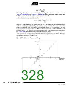
tive. Figure 25-14 shows the decoding of the differential input range.
Table 82 shows the resulting output codes if the differential input channel pair (ADCn - ADCm) is
selected with a reference voltage of VREF
.
Figure 25-14. Differential Measurement Range
Output Code
0x1FF
0x000
0
Differential Input
Voltage (Volts)
- VREF
VREF
0x3FF
0x200
328
AT90USB64/128
7593A–AVR–02/06

 ATMEL [ ATMEL ]