AT90USB64/128
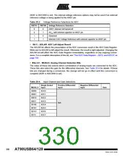
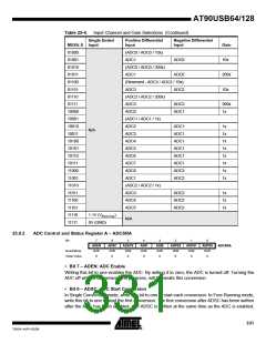
Table 25-4. Input Channel and Gain Selections (Continued)
Single Ended
MUX4..0 Input
Positive Differential
Input
Negative Differential
Input
ADC0
ADC0
Gain
10x
01000
01001
01010
01011
01100
01101
01110
01111
10000
10001
10010
10011
10100
10101
10110
10111
11000
11001
11010
11011
11100
11101
11110
11111
(ADC0 / ADC0 / 10x)
ADC1
(ADC0 / ADC0 / 200x)
ADC1
200x
10x
(Reserved - ADC2 / ADC2 / 10x)
ADC3
ADC2
(ADC2 / ADC2 / 200x)
ADC3
ADC2
ADC1
200x
1x
ADC0
(ADC1 / ADC1 / 1x)
ADC2
ADC1
ADC1
ADC1
ADC1
ADC1
ADC1
ADC2
ADC2
1x
1x
1x
1x
1x
1x
1x
1x
N/A
ADC3
ADC4
ADC5
ADC6
ADC7
ADC0
ADC1
(ADC2 / ADC2 / 1x)
ADC3
ADC2
ADC2
ADC2
1x
1x
1x
ADC4
ADC5
1.1V (VBand Gap
0V (GND)
)
N/A
25.8.2
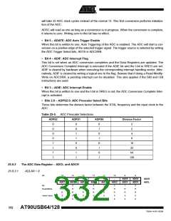
ADC Control and Status Register A – ADCSRA
Bit
7
ADEN
R/W
0
6
ADSC
R/W
0
5
ADATE
R/W
0
4
ADIF
R/W
0
3
ADIE
R/W
0
2
1
ADPS1
R/W
0
0
ADPS0
R/W
0
ADPS2
ADCSRA
Read/Write
Initial Value
R/W
0
• Bit 7 – ADEN: ADC Enable
Writing this bit to one enables the ADC. By writing it to zero, the ADC is turned off. Turning the
ADC off while a conversion is in progress, will terminate this conversion.
• Bit 6 – ADSC: ADC Start Conversion
In Single Conversion mode, write this bit to one to start each conversion. In Free Running mode,
write this bit to one to start the first conversion. The first conversion after ADSC has been written
after the ADC has been enabled, or if ADSC is written at the same time as the ADC is enabled,
331
7593A–AVR–02/06

 ATMEL [ ATMEL ]