AT89C5132
23.2.4
Oscillator and Crystal
23.2.4.1
Schematic
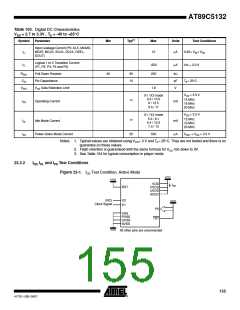
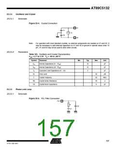
Figure 23-4. Crystal Connection
X1
X2
C1
C2
Q
VSS
Note:
For operation with most standard crystals, no external components are needed on X1 and X2. It
may be necessary to add external capacitors on X1 and X2 to ground in special cases (max 10
pF). X1 and X2 may not be used to drive other circuits.
23.2.4.2
Parameters
Table 105. Oscillator and Crystal Characteristics
DD = 2.7 to 3.3V , TA = -40 to +85°C
V
Symbol
CX1
CX2
CL
Parameter
Min
Typ
10
10
5
Max
Unit
pF
Internal Capacitance (X1 - VSS
Internal Capacitance (X2 - VSS
)
)
pF
Equivalent Load Capacitance (X1 - X2)
Drive Level
pF
DL
50
20
40
6
µW
MHz
Ω
F
Crystal Frequency
RS
Crystal Series Resistance
Crystal Shunt Capacitance
CS
pF
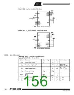
23.2.5
Phase Lock Loop
23.2.5.1
Schematic
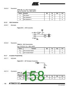
Figure 23-5. PLL Filter Connection
FILT
R
C2
C1
VSS
VSS
157
4173E–USB–09/07

 ATMEL [ ATMEL ]