AT89C5132
Table 103. Digital DC Characteristics
VDD = 2.7 to 3.3V , TA = -40 to +85°C
Symbol
Parameter
Min
Typ(1)
Max
Units
Test Conditions
Input Leakage Current (P0, ALE, MCMD,
MDAT, MCLK, SCLK, DCLK, DSEL,
DOUT)
ILI
10
µA
0.45< VIN< VDD
Logical 1 to 0 Transition Current
(P1, P2, P3, P4 and P5)
ITL
-650
200
µA
Vin = 2.0 V
RRST
CIO
Pull-Down Resistor
Pin Capacitance
50
90
10
kΩ
pF
V
TA= 25°C
VRET
VDD Data Retention Limit
1.8
VDD < 3.3 V
X1 / X2 mode
6.5 / 10.5
8 / 13.5
12 MHz
16 MHz
20 MHz
(3)
IDD
Operating Current
mA
9.5 / 17
V
DD < 3.3 V
X1 / X2 mode
5.3 / 8.1
12 MHz
16 MHz
20 MHz
(3)
IDL
Idle Mode Current
mA
6.4 / 10.3
7.5 / 13
IPD
Power-Down Mode Current
20
500
µA
VRET < VDD < 3.3 V
Notes: 1. Typical values are obtained using VDD= 3 V and TA= 25°C. They are not tested and there is no
guarantee on these values.
2. Flash retention is guaranteed with the same formula for VDD min down to 0V.
3. See Table 154 for typical consumption in player mode.
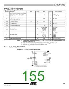
23.2.2
IDD, IDL and IPD Test Conditions
Figure 23-1. IDD Test Condition, Active Mode
VDD
VDD
VDD
PVDD
UVDD
AVDD
IDD
RST
(NC)
Clock Signal
X2
X1
VDD
P0
VSS
PVSS
UVSS
AVSS
TST
VSS
All other pins are unconnected
155
4173E–USB–09/07

 ATMEL [ ATMEL ]