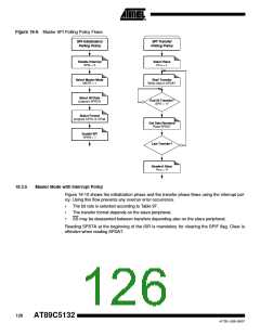
In case of the AT89C5132 is the only slave on the bus, it can be useful not to use SS pin and get
it back to I/O functionality. This is achieved by setting SSDIS bit in SPCON. This bit has no effect
when CPHA is cleared (see Section "SS Management", page 123).
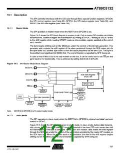
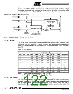
Figure 19-4. SPI Slave Mode Block Diagram
MISO/P4.2
I
Q
MOSI/P4.1
8-bit Shift Register
SPDAT WR
SPDAT RD
SCK/P4.2
SS/P4.3
Control and Clock Logic
SPIF
SPSTA.7
SSDIS
SPCON.5
CPHA
SPCON.2
CPOL
SPCON.3
Note:
MSTR bit in SPCON is cleared to select slave mode.
19.1.3
Bit Rate
The bit rate can be selected from seven predefined bit rates using the SPR2, SPR1 and SPR0
control Bits in SPCON according to Table 97. These bit rates are derived from the peripheral
clock (FPER) issued from the Clock Controller block as detailed in Section “Clock Controller”,
page 12.
Table 97. Serial Bit Rates
Bit Rate (kHz) Vs FPER
SPR2 SPR1 SPR0 6 MHz(1) 8 MHz(1) 10 MHz(1) 12 MHz(2) 16 MHz(2) 20 MHz(2)
FPER Divider
0
0
0
0
1
1
1
1
0
0
1
1
0
0
1
1
0
1
0
1
0
1
0
1
3000
1500
750
4000
2000
1000
500
5000
2500
6000
3000
1500
750
8000
4000
2000
1000
500
10000
5000
2
4
1250
2500
8
375
625
1250
16
32
64
128
1
187.5
93.75
46.875
6000
250
312.5
156.25
78.125
10000
375
625
125
187.5
93.75
12000
250
312.5
156.25
20000
62.5
8000
125
16000
Notes: 1. These frequencies are achieved in X1 mode, FPER = FOSC ÷ 2.
2. These frequencies are achieved in X2 mode, FPER = FOSC
.
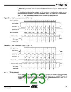
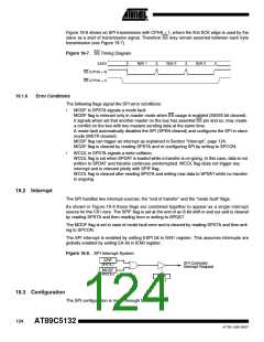
19.1.4
Data Transfer
The Clock Polarity bit (CPOL in SPCON) defines the default SCK line level in idle state(1) while
the Clock Phase bit (CPHA in SPCON) defines the edges on which the input data are sampled
and the edges on which the output data are shifted (see Figure 19-5 and Figure 19-6). The SI
signal is output from the selected slave and the SO signal is the output from the master. The
122
AT89C5132
4173E–USB–09/07

 ATMEL [ ATMEL ]