AT8xC51SND2C
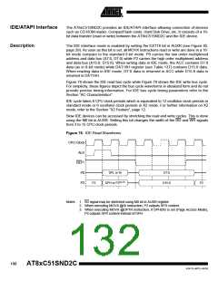
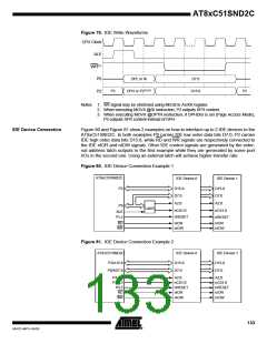
Figure 79. IDE Write Waveforms
CPU Clock
ALE
WR(1)
DPL or Ri
D7:0
P0
P2
P2
DPH or P2(2),(3)
D15:8
P2
Notes: 1. WR signal may be stretched using M0 bit in AUXR register.
2. When executing MOVX @Ri instruction, P2 outputs SFR content.
3. When executing MOVX @DPTR instruction, if DPHDIS is set (Page Access Mode),
P2 outputs SFR content instead of DPH.
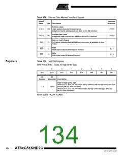
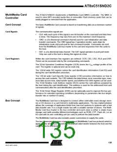
IDE Device Connection
Figure 80 and Figure 81 show 2 examples on how to interface up to 2 IDE devices to the
AT8xC51SND2C. In both examples P0 carries IDE low order data bits D7:0, P2 carries
IDE high order data bits D15:8, while RD and WR signals are respectively connected to
the IDE nIOR and nIOW signals. Other IDE control signals are generated by the exter-
nal address latch outputs in the first example while they are generated by some port
I/Os in the second one. Using an external latch will achieve higher transfer rate.
Figure 80. IDE Device Connection Example 1
AT8xC51SND2C
P2
IDE Device 0
IDE Device 1
D15-8
D7:0
A2:0
D15-8
D7:0
A2:0
P0
Latch
nCS1:0
nCS1:0
ALE
Px.y
nRESET
nRESET
RD
nIOR
nIOW
nIOR
nIOW
WR
Figure 81. IDE Device Connection Example 2
AT8xC51SND2C
IDE Device 0
IDE Device 1
P2/A15:8
P0/AD7:0
D15-8
D7:0
D15-8
D7:0
P4.2:0
P4.4:3
P4.5
RD
A2:0
A2:0
nCS1:0
nRESET
nIOR
nCS1:0
nRESET
nIOR
WR
nIOW
nIOW
133
4341D–MP3–04/05

 ATMEL [ ATMEL ]