AT8xC51SND2C
Description
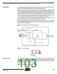
The USB device controller provides the hardware that the AT8xC51SND2C needs to
interface a USB link to a data flow stored in a double port memory.
It requires a 48 MHz reference clock provided by the clock controller as detailed in Sec-
tion "", page 103. This clock is used to generate a 12 MHz Full Speed bit clock from the
received USB differential data flow and to transmit data according to full speed USB
device tolerance. Clock recovery is done by a Digital Phase Locked Loop (DPLL) block.
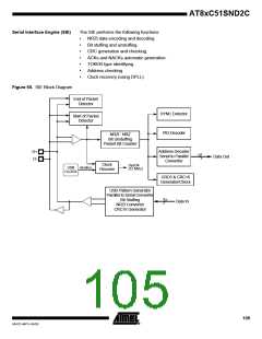
The Serial Interface Engine (SIE) block performs NRZI encoding and decoding, bit stuff-
ing, CRC generation and checking, and the serial-parallel data conversion.
The Universal Function Interface (UFI) controls the interface between the data flow and
the Dual Port RAM, but also the interface with the C51 core itself.
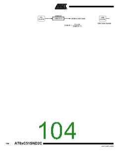
Figure 64 shows how to connect the AT8xC51SND2C to the USB connector. D+ and D-
pins are connected through 2 termination resistors. Value of these resistors is detailed in
the section “DC Characteristics”.
Figure 62. USB Device Controller Block Diagram
USB
CLOCK
48 MHz
12 MHz
DPLL
D+
D-
USB
Buffer
To/From
C51 Core
UFI
SIE
Figure 63. USB Connection
To Power Supply
VBUS
RUSB
RUSB
D+
D-
D+
D-
GND
VSS
Clock Controller
The USB controller clock is generated by division of the PLL clock. The division factor is
given by USBCD1:0 bits in USBCLK register (see Table 135). Figure 64 shows the USB
controller clock generator and its calculation formula. The USB controller clock fre-
quency must always be 48 MHz.
Figure 64. USB Clock Generator and Symbol
103
4341D–MP3–04/05

 ATMEL [ ATMEL ]