AT7908E
Detailed Pin Description
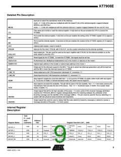
Input pin to select the operational mode of the interface:
mode = 0 : 8 bits of the data bus multiplexed with the lowest 8 bits of the address(register mapped between
8000Hex and 804Chex)
MODE
CS
mode = 1 : 8 bits not multiplexed with the address data bus ( register mapped between 00 Hex and 4C Hex)
Chip select pin to write or read the internal register. A high level on this pin enables the CPU to access the
AT7908E.
Pin to write the internal register. A low level on this pin enables the writing of the AT7908E register (if CS signal is
HIGH).
WR
Pin to read the internal register. A low level on this pin enables the readout of the AT7908E register (if CS signal is
HIGH).
RD
ALE
Address-latch-enable. Used in mode=0.
XTALIN
Input pin for the clock. XTALIN, with XTALOUT, are the crystal connections for the internal oscillator.
Input output pin. This pin could be used as the input, together with XTALIN, for the internal oscillator or as the
clock output to drive the CPU.
XTALOUT
RESET
Reset signal for the AT7908E. To reset the AT7908E, this signal must be set low.
Bi-directional bus: Multiplexed data/address bus in the mode 0 or data bus in the mode1.
Highest input address in the mode0 or lowest input address in the mode 1.
DATA<7:0>
ADDR<7:0>
Output pin for the interrupt request to the MCU. This pin is active low (interrupt generation) and will be kept low
until the MCU clears the interrupt request on AT7908E.
INT
CAN_TX
CAN_RX
Serial output pin to the CAN transceiver (dominant=‘0’, recessive=‘1’)
Serial input from the CAN transceiver (dominant=‘0’, recessive=‘1’).
Input signal to enable the scan-test (with test = 1) or to put the AT7908E on power down mode (with test signal =
0). To use the AT7908E in normal functional mode, this signal must be logical 0.
SENA
TEST
Input signal to increase the testability. This pin will be used in the test modality. Test = 1 => test mode (used by the
manufacturer that executes the test of the device. Test = 0 => functional mode ( if SENA =0) or power down
mode ( if SENA =1).
Output signal that will be set high (duration of the pulse = 13 clock cycles) if the received message arbitration
matches the TRIGGER_MATCH register (independently from the matching between the arbitration of the
incoming message and the identifier of the message buffers). This pin could be used for the bus switching in a
system with two physical buses (nominal and redundant).
HATRIG
Output signal that could be used to advise that the node started to transmit a message or started to receive a
message (duration of the pulse = 13 clock cycles).
HASYNC
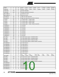
Internal Register
Description
Type
R = read
R/W =
Address
Register Name
read/write
Hex
Register function ( bit7… bit0)
Gensync
Tx
Gensync
Rx
R/W
00
BPR1
BPR0
Errint
Overint
Rxint
Txint
SETUP_0
SETUP_1
SETUP_2
SETUP_3
SETUP_RX
R/W
R/W
R/W
R/W
01
02
03
04
Disabled
PS2_3
TXRM
PS2_2
Reset
TXEM
PS2_1
IntClr
TMRMR
PS2_0
AbortTx
Reserved
TXDLC3
PS1_3
TXDLC1
PS1_2
RSJ2
TXDLC1
PS1_1
RSJ1
TXDLC0
PS1_0
RSJ0
RxClr
Txreq
reserved
reserved
reserved
reserved
Rxclr3
Rxclr2
Rxclr1
9
4268D–AERO–11/09

 ATMEL [ ATMEL ]