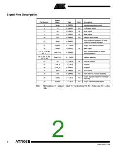
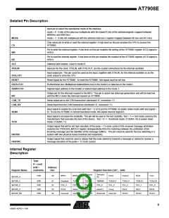
Signal Pins Description
Signal
Name
Pin Number
Type
Note
Description
9
Mode
Cs
I - CMOS
I - CMOS
I - CMOS
I - CMOS
I - CMOS
Interface operational mode
Chip select signal
Write signal
8
AH
AL
AL
AH
11
13
10
Wr
Rd
Read signal
ALE
Address latch enable
Input to internal oscillators or clock
input from external oscillator
23
Xtalin
I - CMOS
22
16
Xtalout
Reset
IO - CMOS
I - CMOS
Output from internal oscillator
reset signal
AL
AL
5, 4, 3, 2, 44, 43,
42, 41
Input address(mode1) or output
address(mode 0)
addr<7:0>
Data<7:0>
I - CMOS
38, 37, 36, 35, 33,
32, 31, 30
IO - CMOS
Address data bus
25
27
19
14
15
Int
O - CMOS
O - CMOS
I - CMOS
I - CMOS
I - CMOS
interrupt request
tx signal
Can_tx
Can_rx
sena
rx signal
AH
AH
scan enable
test
input signal to increase testability
Output signal to trigger the message
matching
26
20
hatrig
O - CMOS
O - CMOS
AH
AH
hasync
Output synchronization signal
Note:
Abbreviations: O = output, I = input, IO = bi-directional I/O, AL = Active Low, AH = Active
High.
2
AT7908E
4268D–AERO–11/09

 ATMEL [ ATMEL ]