AT7908E
RXn_Message_6: seventh 8 bits data of the message object n
RXn_Message_7: eighth 8 bits data of the message object n
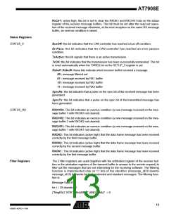
The following bit composes the RXn_STATUS register of the message buffer:
RXn_DLC3:RXn_DLC0: length of the received message
(length = RXn_DLC0 +2 x RXn_DLC1 + 4 x RXn_DLC2 + 8 x RXn_DLC3)
RXn_extfr: if this bit is high, the received message has an extended identifier.
Error Counters Registers
Trigger Match Registers
The AT7908E has two internal counters for the RX and TX errors. The values of these
counters are stored into two registers that can be read from the MCU.
The Trigger Match registers are implemented to generate a pulse on the HATRIG output
signal when the received message arbitration match the Trigger Match registers (see
the trigger match functionality).
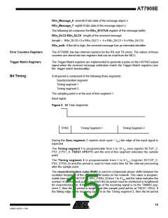
Bit Timing
A bit period is composed of the following three segments:
Synchronization segment
Timing segment 1
Timing segment 2
The sampling point is at the end of time segment 1.
Input signal
Figure 2. Bit Time Segments
SYNC
Timing Segment 1
Timing Segment 2
During the Sync segment (1 system clock cycle = tscl) the edge of the input signal is
expected.
The Timing segment 1 is programmable from 2 to 16 tscl (see register SETUP_2:
PS1_3:PS1_0: TSEG1 =PS1+1) and the end of this segment indicates the sample
point.
The Timing segment 2 is programmable from 1 to 8 tscl (register SETUP_2:
PS2_3:PS2_0) and this period is used to have extra time for the internal processing
after the sample point.
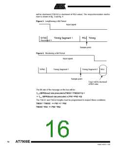
The resynchronization Jump Width is used to compensate phase shifts between the
oscillator frequency of the different CAN nodes on the network. This value is program-
mable (see register SETUP_3: RSJ_2:RSJ_0) from 1 to 4 tscl and the value indicates the
number of system clock pulses by which the bit period must be shortened or lengthened
for resynchronization. If the falling edge of the incoming signal is on the TIMING seg-
ment 1, then the Bit period is lengthened (the sample point will be at TSEG1 +RSJ). If
the falling edge of the incoming signal is on the Timing segment 2, then the bit period
15
4268D–AERO–11/09

 ATMEL [ ATMEL ]