AT7908E
Interface Block
Description
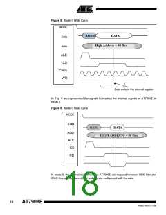
The AT7908E provides a programmable (with external pin) MCU interface. Two modes
can be selected. The first operational mode is an interface with 8-bit multiplexed
address data bus (mode = 0) and an internal register addressable with 16-bit of address.
In this operational mode, the AT7908E registers are mapped between 8000Hex and
804CHex.
The second operational mode (mode =1) is implemented with 8 bit not multiplexed
address and data buses. In this mode the internal registers are accessible with 8-bit and
are mapped between 00Hex and 4C Hex.
The pins for the interface block are:
Selection of the interface modality. This pin must be 0 to use 8 bits
multiplexed data address (lowest) to map the AT7908E on the highest
address space (8000Hex to 804C Hex). If MODE = 1, the data and
addresses are not multiplexed and the registers are mapped on the lowest
Mode
Data <7:0>
ALE
address space.
bi-directional 8-bit address (low address in mode 0) data bus
Input Address Latch Enable used for mode 0.
CS
Input Chip select to enable the internal registers access (active high).
Input Write signal to write the internal registers (active low).
Input Read signal to readout the internal registers (active low).
WR
RD
Input highest address in mode 0 (used with low address to map the
AT7908E register between 8000Hex and 804Chex address space) or input
lowest address in mode 1
Addr <7:0>
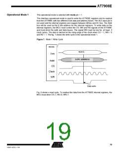
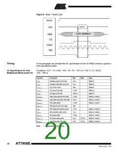
Operational Mode 0
This operational mode is selected with MODE pin = 0.
The bus Data_addr <7:0> must be connected to the data/address bus of the MCU. The
ALE signal is used to latch the address. This latched address will be the address of the
AT7908E internal registers. The bus addr (7:0) will contain the highest address gener-
ated by the MCU. The internal AT7908E registers will be accessed only if the 16-bit
address generated by the MCU is between 8000 Hex and 804C Hex (the internal Chip
Select will be generated). Moreover, to write in the register or to read from the register,
the micro-controller must generate the CS (active high), WR, RD and ALE signals and
must drive the Data_addr and addr buses. The signal WR must be low for, at least, 3
clock cycles. The data is latched at the rising edge of the clock when CS = 1, WR = 0
and RD = 1.
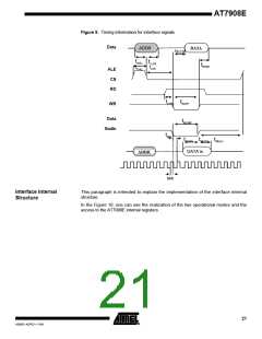
A write cycle is reported in Fig. 5.
17
4268D–AERO–11/09

 ATMEL [ ATMEL ]