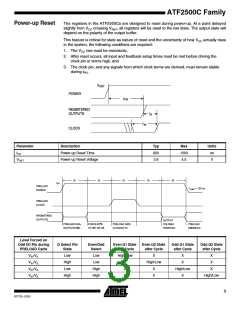
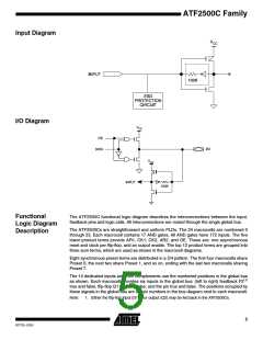
ATF2500C Family
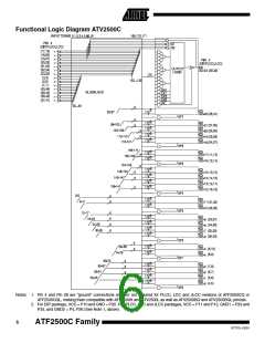
Output Logic, Registered(1)
S2 = 0
Terms in
S1
0
S0
0
D/T1
D/T2
4
Output Configuration
Registered (Q1); Q2 FB
Registered (Q1); Q2 FB
Registered (Q1); D/T2 FB
8
12
8
1
0
4(1)
4
1
1
Output
S3
0
Configuration
S6
0
Q1 CLOCK
CK1
CK1 • PIN1
Active Low
1
Active High
1
Q2 CLOCK
S4
0
Register 1 Type
S7
0
D
T
CK2
1
1
CK2 • PIN1
S5
0
Register 2 Type
D
T
1
Output Logic, Combinatiorial(1)
S2 = 1
S1
Terms in
S5
S0
D/T1
4(1)
D/T2
Output Configuration
Combinatorial (8 Terms);
Q2 FB
X
X
X
1
0
0
1
1
1
0
4
Combinatorial (4 Terms);
Q2 FB
1
0
1
1
4
4
4(1)
4
Combinatorial (12 Terms);
Q2 FB
4(1)
4(1)
4
Combinatorial (8 Terms);
D/T2 FB
Combinatorial (4 Terms);
D/T2 FB
0
4
Note:
1. These four terms are shared with D/T1.
Clock Option
Note:
1. These diagrams show equivalent logic functions, not
necessarily the actual circuit implementation.
7
0777G–12/01

 ATMEL [ ATMEL ]