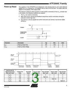
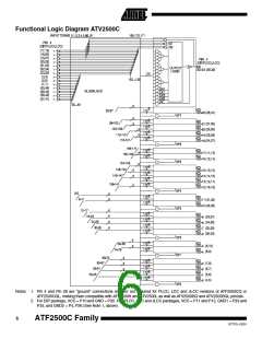
Preload and
Observability of
Registered
Outputs
The ATF2500Cs registers are provided with circuitry to allow loading of each register asyn-
chronously with either a high or a low. This feature will simplify testing since any state can be
forced into the registers to control test sequencing. A VIH level on the odd I/O pins will force the
appropriate register high; a VIL will force it low, independent of the polarity or other configura-
tion bit settings.
The PRELOAD state is entered by placing an 10.25V to 10.75V signal on SMP lead 42. When
the preload clock SMP lead 23 is pulsed high, the data on the I/O pins is placed into the 12
registers chosen by the Q select and even/odd select pins.
Register 2 observability mode is entered by placing an 10.25V to 10.75V signal on pin/lead 2.
In this mode, the contents of the buried register bank will appear on the associated outputs
when the OE control signals are active.
Programming
Software
Support
All family members of the ATF2500C can be designed with Atmel-Synario™ and Atmel-Win-
CUPL™. ProChip™ designer support will be available Q102.
Additionally, the ATF2500C may be programmed to perform the ATV2500H/Ls functional sub-
set (no T-type flip-flops, pin clocking or D/T2 feedback) using the ATV2500H/L JEDEC file. In
this case, the ATF2500C becomes a direct replacement or speed upgrade for the
ATV2500H/L. The ATF2500CQ/CQL are direct replacements for the ATV2500BQ/BQL and
the AT2500H/L, including the lack of extra grounds on P4 and P26.
Security Fuse
Usage
A single fuse is provided to prevent unauthorized copying of ATF2500C fuse patterns. Once
programmed, the outputs will read programmed during verify.
The security fuse should be programmed last, as its effect is immediate.
The security fuse also inhibits Preload and Q2 observability.
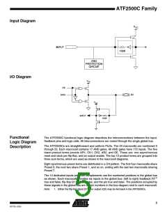
Input and I/O
Pull-ups
All ATF2500C family members have programmable internal input and I/O pinkeeper circuits.
The default condition, including when using the AT2500CQ/CQL family to replace the
AT2500BQ/BQL or AT2500H/L, is that the pinkeepers are not activated.
When pinkeepers are active, inputs or I/Os not being driven externally will maintain their last
driven state. This ensures that all logic array inputs and device outputs are known states.
Pinkeepers are relatively weak active circuits that can be easily overridden by TTL-compatible
drivers (see input and I/O diagrams below).
4
ATF2500C Family
0777G–12/01

 ATMEL [ ATMEL ]