Absolute Maximum Ratings*
*NOTICE:
Stresses beyond those listed under “Absolute
Maximum Ratings” may cause permanent dam-
age to the device. This is a stress rating only and
functional operation of the device at these or any
other conditions beyond those indicated in the
operational sections of this specification is not
implied. Exposure to absolute maximum rating
conditions for extended periods may affect device
reliability.
Temperature Under Bias................................ -55°C to +125°C
Storage Temperature..................................... -65°C to +150°C
Junction Temperature .............................................150°C Max
Voltage on Any Pin with
Respect to Ground .........................................-2.0V to +7.0V(1)
Voltage on Input Pins
Note:
1. Minimum voltage is -0.6V DC which may under-
shoot to -2.0V for pulses of less than 20 ns.
Maximum output pin voltage is VCC + 0.75V DC
which may overshoot to +7.0V for pulses of less
than 20 ns.
with Respect to Ground
During Programming.....................................-2.0V to +14.0V(1)
Programming Voltage with
Respect to Ground .......................................-2.0V to +14.0V(1)
DC and AC Operating Conditions
Commercial
Industrial
Military
0°C - 70°C
-40°C - 85°C
(Ambient)
-55°C - 125°C
(Case)
Operating Temperature
(Ambient)
VCC Power Supply
5V 5%
5V 10%
5V 10%
Pin Capacitance
f = 1 MHz, T = 25°C(1)
Typ
4
Max
6
Units
Conditions
CIN
pF
VIN = 0V
COUT
8
12
pF
VOUT = 0V
Note:
1. Typical values for nominal supply voltage. This parameter is only sampled and is not 100% tested.
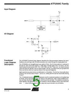
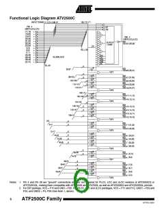
Test Waveforms and Measurement Levels Output Test Load
8
ATF2500C Family
0777G–12/01

 ATMEL [ ATMEL ]