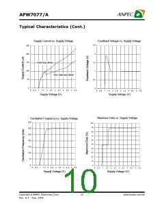
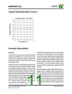
APW7077/A
Function Description (Cont.)
Inductor Selection (Cont.)
If the regulator will be loaded uniformly, with very little
load changes, and at lower current outputs, the input
capacitor size canoften be reduced. The size can also
be reduced if the input of the regulator is very close to
the source output. The size will generally need to be
larger for applicationswherethe regulator issupplying
nearly the maximum ratedoutput or if large load steps
are expected. A minimum value of 10µF should be
used for the less stressful conditions while a 22µF to
47µF capacitor may be required for higher power and
dynamic loads. Small ESR Tantalum or ceramic ca-
pacitor should be suitable and the total input ripple
voltage canbe calculated
when DIL is less than the average inductor current.
Care must be taken to make sure that the switch will
not reach its current limit during normal operation.
The inductor must also be sized accordingly. It should
have a saturation current rating higher than the peak
inductor current expected. The output voltage ripple is
also affected by the total ripple current.
Output Capacitor
The output capacitor is used for sustaining the output
voltage when the external MOSFET or bipolar
transistor is switched on and smoothing the ripple
voltage.
DVIN = DIL ´ ESR
Design Example
The output capacitance needed is calculated in
equations.
It is supposed that a step–up DC–DC controller with
3.3 V output delivering a maximum 1000 mA output
current with 100 mV output ripple voltage powering
from a 2.4 V input is to be designed.
IO(max) ´ D
COUT(min) =
fsw ´ DVOUT
The ESR is also important because it determines the
peak to peak output voltage ripple according to the
approximateequation:
Design parameters:
VIN = 2.4 V
?V
OUT
VOUT = 3.3 V
ESR =
?I
O
IO = 1.0 A
With 1% output voltage ripple, low ESR capacitor
should be used to reduce output ripple voltage. In
DVOUT = 100 mV
fsw= 300 kHZ
general, a 100uF to 220uF low ESR (0.10W to 0.30W)
Tantalum capacitor should be appropriate. The choice
of output capacitors is also somewhat arbitrary and
dependson the designrequirementsfor output voltage
ripple.Aminimum value of 10µF isrecommended and
may be increased to a larger value.
Ratio = 0.2 (typical for small output ripple voltage)
Assume the diode forward voltage and the transistor
saturation voltageare both 0.3V. Determine the maxi-
mum steady state duty cycle at VIN = 2.4 V:
D=0.273
Calculate the maximum inductance value which can
generate the desired current output and the preferred
deltainductor current to averageinductor current ratio:
Input Capacitor
The input capacitor can stabilize the input voltage and
minimize peak current ripplefrom the source. Thesize
usedis dependant on the applicationand board layout.
L=10uH
Copyright ã ANPEC Electronics Corp.
14
www.anpec.com.tw
Rev. A.4 - Sep, 2005

 ANPEC [ ANPEC ELECTRONICS COROPRATION ]