APW7077/A
Function Description (Cont.)
Operation (Cont.)
ramp up to let output voltage reach to setting voltage
without over shooting issue whenever heavy load or
light load condition. The soft start time 25ms is
setting by internal circuit.
inductor current ishigher than the output current, then
sustains the output voltage until the next switching
cycle.
Oscillator
As the load current is decreased, the switch transistor
turns on for a shorter duty cycle. Under the light load
condition, the controller will skip switching cycles to
reduce power consumption, so that high efficiency is
maintained at light loads.
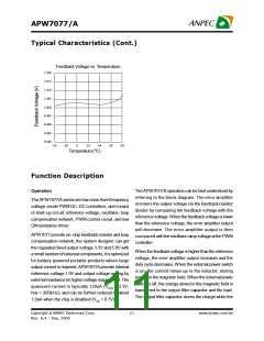
The oscillator frequency is internally set to 300 kHz at
an accuracy of +/-10% and with low temperature
coefficient of 3.3%/°C.
Enable/Disable Operation
Fixed Output Voltage (for APW7077 only)
TheAPW7077/Aseriesoffer IC shutdown modebychip
enable pin (CE pin) to reduce current consumption.
When voltage at pin CE is greater than 1.2 V, the
chip will be enabled, which means the controller is
in normal operation. When voltage at pin CE is less
than 0.7 V, the chip is disabled, which means IC is
shutdown and quiescent current become 1uA.
The APW7077 VOUT is set by an integrate feedback
resistor network. This is trimmed to a selected voltage
3.3 V or 5.0 V with an accuracy of +/-2.5%.
Setting Output Voltage (for APW7077A only)
For APW7077A, the output voltage is adjustable. The
output voltage is set using the FB pin and a resistor
divider connected to the output as shown in the typical
operating circuit. The internal reference voltage is1.0V
with 2% variation, so the ratio of the feedback resistors
sets the output voltage according to the following
The CE pin pull hightoVDD(or VOUT) by internal resistor,
and this resistance is greater than 1MW . So this chip
will enable normally when CE pin floating.
Important: DO NOT apply a voltage between 0.7V
to 1.2 V to pin CE as this is the CE pin’s hysteresis
voltage range. Clearly defined output states can
only be obtained by applying voltage out of this
range.
equation:
R2
VOUT = (1 +
) ´ 1.0V
R1
To avoid the thermal noise from feedback resistor,
(R1+R2) resistance smaller than 1MW and 1%variation
isrecommended.
Compensation
The device is designed to operate in continuous
conduction mode. An internal compensation circuit
was designed to guarantee stability over the full
input/output voltage and full output load range.
Soft Start
There is a soft start function is integration in
APW7077/A series to avoid the over shooting when
power on. When power is applied to the device, the
soft start circuit first pumps up the output voltage to
Step–up Converter Operating Mode
let VDD(or VOUT) approximately 1.65V at a fixed duty The step–upDC–DC controller isdesigned to operate
in continuous conduction mode (CCM) or discontinuous
cycle 50%. This is the voltage level at which the
controller can operate normally. When supply voltage conduction mode (DCM).
more than 1.65Vthe internal reference voltage will be
For a step up converter in a CCM, the duty cycle D is
Copyright ã ANPEC Electronics Corp.
12
www.anpec.com.tw
Rev. A.4 - Sep, 2005

 ANPEC [ ANPEC ELECTRONICS COROPRATION ]