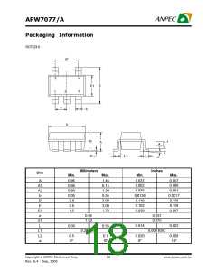
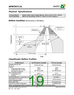
APW7077/A
External Component Selection (Cont.)
transistor. Moreover, aspeed–upcapacitor, Cb, should
External Switch Transistor (Cont.)
be connected in parallel with Rb to reduce switching
loss and improve efficiency. Cb can be calculated by
the equation below:
the controller’s EXT pin must be able to supply the
necessary driving current. Rb can be calculated by
the following equation:
It is due to the variation in the characteristics of the
transistor used. The calculated value should be used
as the initial test value and the optimized value should
be obtained by the experiment.
Since the pulse current flows through the transistor,
the exact Rb value should be finely tuned by the
experiment. Generally, a small Rb value can increase
the output current capability, but the efficiency will
decrease due to more energy is used to drive the
Layout Considerations
Ground Plane
Switching Noise Decoupling Capacitor
One point grounding should be used for the output
power return ground, the input power return ground,
and the device switch ground to reduce noise. The
input ground and output ground traces must be thick
enough for current to flow through and for reducing
ground bounce.
On APW7077 fixed voltage application, a 0.1mF ce-
ramic capacitor should be placed close to the VOUT pin
and GND pin of the chip to filter the switching spikes
in the output voltage monitored by the VOUT pin.
Feedback Network
On APW7077A application, the feedback networks
should be connected directly to a dedicated analog
ground plane and this ground plane must connect to
the GND pin. If no analog ground plane is available
then this ground must tie directly to the GNDpin. The
feedback network, resistorsR1 and R2, should bekept
close to the FB pin, and away from the inductor, to
minimizecoppertraceconnectionsthat caninject noise
into the system.
Power Signal Traces
Low resistance conducting paths should be used for
the power carrying traces to reduce power loss so as
to improve efficiency (short and thick traces for con-
necting the inductor L can also reduce stray
inductance). Trace connections made to the inductor
and schottky diode should be minimized to reduce
power dissipation and increase overall efficiency.
Output Capacitor
Input Capacitor
The output capacitor should be placed close to the
output terminals to obtain better smoothing effect on
the output ripple.
InAPW7077A high output voltage application circuit,
the input voltage(VIN) is tied to chip supply pin(VDD).
The input capacitor CIN in VIN must be placed close to
the IC. This will reduce copper trace resistance which
effects input voltage ripple of the IC. For additional
The output capacitor, COUT, shouldalsobeplaced close
to the IC. Any copper trace connections for the COUT
capacitor can increase the series resistance, which
directly effects output voltage ripple and efficiency.
input voltage filtering, a 1mF capacitor can be placed
in parallel with CIN, close to the VDD pin, to shunt any
high frequency noise to ground.
Copyright ã ANPEC Electronics Corp.
16
www.anpec.com.tw
Rev. A.4 - Sep, 2005

 ANPEC [ ANPEC ELECTRONICS COROPRATION ]