APW7077/A
Typical Characteristics (Cont.)
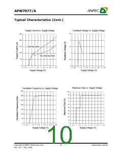
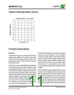
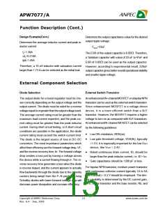
Feedback Voltage vs. Temperature
1.020
1.015
1.010
1.005
1.000
0.995
0.990
0.985
0.980
-40
-20
0
2 0
4 0
60
8 0
Temperature(°C)
Function Description
Operation
TheAPW7077/Aoperation can be best understood by
referring to the block diagram. The error amplifier
monitors the output voltage via the feedback resistor
divider by comparing the feedback voltage with the
referencevoltage.Whenthefeedbackvoltageislower
than the reference voltage, the error amplifier output
will decrease. The error amplifier output is then
compared withtheoscillatorrampvoltageatthePWM
controller.
TheAPW7077/Aseriesare low noise fixed frequency
voltage–mode PWM DC–DC controllers, and consist
of start–up circuit, reference voltage, oscillator, loop
compensation network, PWM control circuit, and low
ONresistance driver.
APW7077provide on–chipfeedback resistor and loop
compensation network, the system designer can get
the regulated fixed output voltage 3.3V and 5.0V with
asmall number of external components, it isoptimized
for battery powered portable products where large
output current is required. APW7077Aprovide internal
reference voltage 1.0V and output voltage setting by
external resistancefor higher voltagerequirement.The
quiescent current is typically 120uA (VOUT = 3.3V,
fsw = 300kHz), and can be further reduced to about
1.0uA when the chip is disabled (VCE < 0.7V).
When thefeedbackvoltageishigherthanthereference
voltage, the error amplifier output increases and the
dutycycle decreases.When theexternal power switch
is on, the current ramps up in the inductor, storing
energyin themagnetic field. Whenthe external power
switch is off, the energy stored in the magnetic field is
transferred to the output filter capacitor and the load.
The output filter capacitor stores the charge while the
Copyright ã ANPEC Electronics Corp.
11
www.anpec.com.tw
Rev. A.4 - Sep, 2005

 ANPEC [ ANPEC ELECTRONICS COROPRATION ]