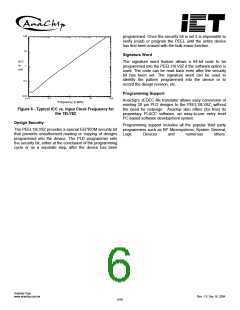
Function Description
The PEEL18LV8Z implements logic functions as sum-of- When programming the PEEL18LV8Z, the device
products expressions in a programmable-AND/fixed-OR programmer first performs a bulk erase to remove the
logic array. Programming the connections of input signals previous pattern. The erase cycle opens every logical
into the array creates user-defined functions. User- connection in the array. The device is configured to
configurable output structures in the form of I/O macrocells perform the user-defined function by programming selected
further increase logic flexibility.
connections in the AND array. (Note that PEEL device
programmers automatically program all of the connections
on unused product terms so that they will have no effect on
the output function).
Architecture Overview
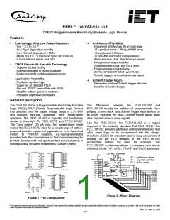
The PEEL18LV8Z architecture is illustrated in the block
diagram of Figure 14. Ten dedicated inputs and 8 I/Os
provide up to 18 inputs and 8 outputs for creation of logic Variable Product Term Distribution
functions. At the core of the device is a programmable
The PEEL18LV8Z provides 113 product terms to drive the
electrically erasable AND array that drives a fixed OR array.
With this structure, the PEEL18LV8Z can implement up to
8 sum-of-products logic expressions.
8 OR functions. These product terms are distributed
among the outputs in groups of 8, 10, 12, 14, and 16 to
form logical sums (see Figure 15). This distribution allows
Associated with each of the 8 OR functions is an I/O optimum use of the device resources.
macrocell that can be independently programmed to one of
12 different configurations. The programmable macrocells
allow each I/O to be used to create sequential or
combinatorial logic functions of active-high or active-low
polarity, while providing three different feedback paths into
the AND array.
Programmable I/O Macrocell
The unique twelve-configuration output macrocell provides
complete control over the architecture of each output. The
ability to configure each output independently lets you to
tailor the configuration of the PEEL18LV8Z to the precise
requirements of your design.
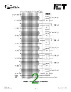
AND/OR Logic Array
The programmable AND array of the PEEL18LV8Z (shown
in Figure 15) is formed by input lines intersecting product
terms. The input lines and product terms are used as
follows:
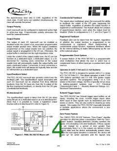
Macrocell Architecture
Each I/O macrocell, as shown in Figure 4, consists of a D-
type flip-flop and two signal-select multiplexers. The four
EEPROM bits controlling these multiplexers determine the
configuration of each macrocell. These bits determine
output polarity, output type (registered or non-registered)
and input-feedback path (bidirectional I/O, combinatorial
feedback). Refer to Table 1 for details.
•
36 Input Lines:
- 20 input lines carry the true and complement of
the signals applied to the 10 input pins
- 16 additional lines carry the true and complement
values of feedback or input signals from the 8
I/Os
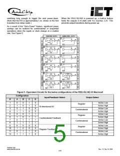
Equivalent circuits for the twelve macrocell configurations
are illustrated in Figure 5. In addition to emulating the four
PAL-type output structures (configurations 3, 4, 9, and 10),
the macrocell provides eight additional configurations.
When creating a PEEL device design, the desired
macrocell configuration is generally specified explicitly in
the design file. When the design is assembled or compiled,
the macrocell configuration bits are defined in the last lines
of the JEDEC programming file.
•
113 product terms:
- 102 product terms are used to form sum of
product functions
- 8 output enable terms (one for each I/O)
- 1 global synchronous preset term
- 1 global asynchronous clear term
- 1 programmable clock term
At each input-line/product-term intersection, there is an
EEPROM memory cell that determines whether or not
there is a logical connection at that intersection. Each
product term is essentially a 36-input AND gate. A product
term that is connected to both the true and complement of
an input signal will always be FALSE and thus will not
affect the OR function that it drives. When all the
connections on a product term are opened, a "don't care"
state exists and that term will always be TRUE.
Output Type
The signal from the OR array can be fed directly to the
output pin (combinatorial function) or latched in the D-type
flip-flop (registered function). The D-type flip-flop latches
data on the rising edge of the clock and is controlled by the
global preset and clear terms. When the synchronous
preset term is satisfied, the Q output of the register is set
HIGH at the next rising edge of the clock input. Satisfying
Anachip Corp.
www.anachip.com.tw
Rev. 1.0 Dec 16, 2004
3/10

 ANACHIP [ ANACHIP CORP ]