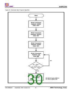
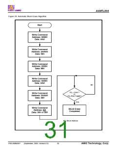
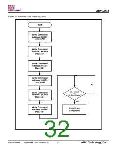
A49FL004
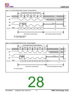
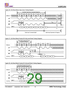
Figure 20: A/A Mux Mode Chip Erase Timing Diagram
Six-Byte Chip Erase Command Sequence
2AAA 5555 5555 2AAA
5555
5555
Address
R/C
OE
TWP TWPH
TSCE
WE
High-Z
AA
55
80
AA
55
10
I/O7-I/O0
Chip Erase Command Input
Chip Erase Operation In Progress
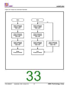
Figure 21: A/A Mux Mode Product ID Entry and Read Timing Diagram
Three-Byte Product ID Entry
Command Sequence
5555
2AAA
5555
0000
0001
0003
Address
R/C
OE
TIDA
TWP TWPH
WE
TAA
High-Z
AA
55
90
37
95
7F
I/O7-I/O0
Figure 22: A/A Mux Mode Product ID Exit and Reset Timing Diagram
Three-Byte Product ID Exit and
Reset Command Sequence
5555
2AAA
5555
Address
R/C
OE
TWP TWPH
WE
High-Z
AA
55
F0
I/O7-I/O0
PRELIMINARY
(September, 2005, Version 0.0)
28
AMIC Technology, Corp.

 AMICC [ AMIC TECHNOLOGY ]