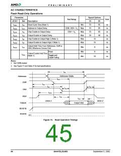
P R E L I M I N A R Y
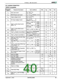
Notes:
1. The ICC current listed is typically less than 2 mA/MHz, with OE# at VIH.
2. Maximum ICC specifications are tested with VCC = VCCmax.
3. ICC active while Embedded Erase or Embedded Program is in progress.
4. Automatic sleep mode enables the low power mode when addresses remain stable for tACC + 30 ns. Typical sleep mode current is
200 nA.
5. Not 100% tested.
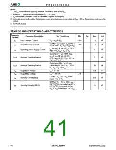
SRAM DC AND OPERATING CHARACTERISTICS
Parameter
Symbol
Parameter Description
Input Leakage Current
Test Conditions
VIN = VSS to VCC
Min
–1.0
–1.0
Typ
Max
1.0
Unit
µA
ILI
CE1#s = VIH, CE2s = VIL or OE# =
VIH or WE# = VIL, VIO= VSS to VCC
ILO
ICC
Output Leakage Current
1.0
µA
IIO = 0 mA, CE1#s = VIL, CE2s =
WE# = VIH, VIN = VIH or VIL
Operating Power Supply Current
3
3
mA
mA
Cycle time = 1 µs, 100% duty,
I
IO = 0 mA, CE1#s ≤ 0.2 V,
CE2 ≥ VCC – 0.2 V, VIN ≤ 0.2 V or
IN ≥ VCC – 0.2 V
ICC1
s
Average Operating Current
Average Operating Current
V
Cycle time = Min., IIO = 0 mA,
100% duty, CE1#s = VIL, CE2s =
VIH, VIN = VIL = or VIH
ICC2s
30
mA
VOL
VOH
Output Low Voltage
Output High Voltage
IOL = 2.1 mA
0.4
V
V
IOH = –1.0 mA
2.4
CE1#s = VIH, CE2 = VIL, Other
inputs = VIH or VIL
ISB
Standby Current (TTL)
0.3
15
mA
CE1#s ≥ VCC – 0.2 V, CE2 ≥ VCC
0.2 V (CE1#s controlled) or CE2 ≤
0.2 V (CE2s controlled), CIOs =
–
ISB1
Standby Current (CMOS)
µA
V
SS or VCC, Other input = 0 ~ VCC
40
Am41DL32x8G
September 5, 2002

 AMD [ AMD ]