PDF
最近搜索
热门搜索
发布采购

| 型号: | M41000002T |
| PDF下载: | 下载PDF文件 查看货源 |
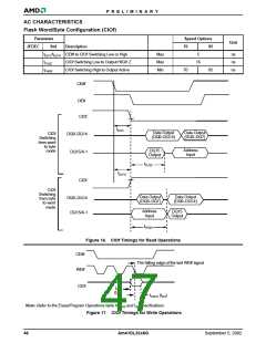
| 内容描述: | 32兆位( 4米×8位/ 2的M× 16位) CMOS 3.0伏只,同步读/写闪存和8兆位( 1一M× 8位/ 512的K× 16位)静态RAM [32 Megabit (4 M x 8-Bit/2 M x 16-Bit) CMOS 3.0 Volt-only, Simultaneous Read/Write Flash Memory and 8 Mbit (1 M x 8-Bit/512 K x 16-Bit) Static RAM] |
| 分类和应用: | 闪存 |
| 文件页数/大小: | 66 页 / 1128 K |
| 品牌: |  AMD [ AMD ] AMD [ AMD ] |
专业IC领域供求交易平台:提供全面的IC Datasheet资料和资讯,Datasheet 1000万数据,IC品牌1000多家。