P R E L I M I N A R Y
ABSOLUTE MAXIMUM RATINGS
OPERATING RANGES
Storage Temperature
Plastic Packages . . . . . . . . . . . . . . . –55°C to +125°C
Industrial (I) Devices
Ambient Temperature (TA) . . . . . . . . .–40°C to +85°C
Ambient Temperature
with Power Applied . . . . . . . . . . . . . . –40°C to +85°C
V
CCf/VCCs Supply Voltage
Voltage with Respect to Ground
V
CCf/VCCs for standard voltage range . . 2.7 V to 3.3 V
V
CCf/VCCs (Note 1) . . . . . . . . . . . .–0.3 V to +4.0 V
Operating ranges define those limits between which the func-
tionality of the device is guaranteed.
RESET# (Note 2) . . . . . . . . . . . .–0.5 V to +12.5 V
WP#/ACC . . . . . . . . . . . . . . . . . .–0.5 V to +10.5 V
All other pins (Note 1). . . . . . –0.5 V to VCC +0.5 V
Output Short Circuit Current (Note 3) . . . . . . 200 mA
Notes:
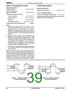
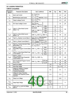
1. Minimum DC voltage on input or I/O pins is –0.5 V.
During voltage transitions, input or I/O pins may
overshoot VSS to –2.0 V for periods of up to 20 ns.
Maximum DC voltage on input or I/O pins is VCC +0.5 V.
See Figure 7. During voltage transitions, input or I/O pins
may overshoot to VCC +2.0 V for periods up to 20 ns. See
Figure 8.
2. Minimum DC input voltage on pins OE#, RESET#, and
WP#/ACC is –0.5 V. During voltage transitions, OE#,
WP#/ACC, and RESET# may overshoot VSS to –2.0 V
for periods of up to 20 ns. See Figure 7. Maximum DC
input voltage on pin RESET# is +12.5 V which may
overshoot to +14.0 V for periods up to 20 ns. Maximum
DC input voltage on WP#/ACC is +9.5 V which may
overshoot to +12.0 V for periods up to 20 ns.
3. No more than one output may be shorted to ground at a
time. Duration of the short circuit should not be greater
than one second.
Stresses above those listed under “Absolute Maximum
Ratings” may cause permanent damage to the device. This
is a stress rating only; functional operation of the device at
these or any other conditions above those indicated in the
operational sections of this data sheet is not implied.
Exposure of the device to absolute maximum rating
conditions for extended periods may affect device reliability.
20 ns
20 ns
20 ns
+0.8 V
VCC
+2.0 V
–0.5 V
–2.0 V
VCC
+0.5 V
2.0 V
20 ns
20 ns
20 ns
Figure 7. Maximum Negative
Overshoot Waveform
Figure 8. Maximum Positive
Overshoot Waveform
38
Am41DL32x8G
September 5, 2002

 AMD [ AMD ]