P R E L I M I N A R Y
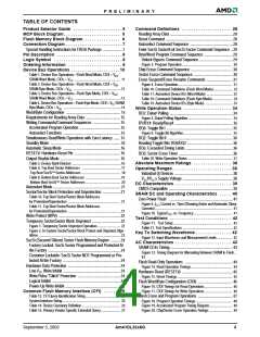
TABLE OF CONTENTS
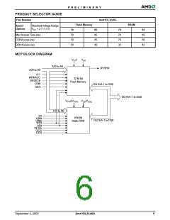
Product Selector Guide . . . . . . . . . . . . . . . . . . . . . 5
MCP Block Diagram. . . . . . . . . . . . . . . . . . . . . . . . 5
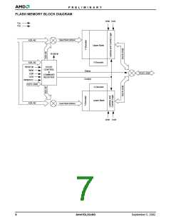
Flash Memory Block Diagram. . . . . . . . . . . . . . . . 6
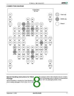
Connection Diagram . . . . . . . . . . . . . . . . . . . . . . . . 7
Special Handling Instructions for FBGA Package ....................7
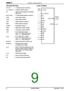
Pin Description . . . . . . . . . . . . . . . . . . . . . . . . . . . . 8
Logic Symbol . . . . . . . . . . . . . . . . . . . . . . . . . . . . . 8
Ordering Information . . . . . . . . . . . . . . . . . . . . . . . 9
Device Bus Operations . . . . . . . . . . . . . . . . . . . . .10
Command Definitions . . . . . . . . . . . . . . . . . . . . . 28
Reading Array Data ................................................................28
Reset Command .....................................................................28
Autoselect Command Sequence ............................................28
Enter SecSi Sector/Exit SecSi Sector Command Sequence ..29
Byte/Word Program Command Sequence .............................29
Unlock Bypass Command Sequence ..................................29
Figure 3. Program Operation ......................................................... 30
Chip Erase Command Sequence ...........................................30
Sector Erase Command Sequence ........................................30
Erase Suspend/Erase Resume Commands ...........................31
Figure 4. Erase Operation.............................................................. 31
Table 16. Command Definitions (Flash Word Mode)...................... 32
Table 17. Autoselect Device IDs (Word Mode) .............................. 32
Table 18. Command Definitions (Flash Byte Mode) ....................... 33
Table 19. Autoselect Device IDs (Byte Mode) ............................... 33
Write Operation Status . . . . . . . . . . . . . . . . . . . . 34
DQ7: Data# Polling .................................................................34
Figure 5. Data# Polling Algorithm .................................................. 34
RY/BY#: Ready/Busy# ............................................................ 35
DQ6: Toggle Bit I ....................................................................35
Figure 6. Toggle Bit Algorithm........................................................ 35
DQ2: Toggle Bit II ...................................................................36
Reading Toggle Bits DQ6/DQ2 ...............................................36
DQ5: Exceeded Timing Limits ................................................36
DQ3: Sector Erase Timer .......................................................36
Table 20. Write Operation Status ................................................... 37
Absolute Maximum Ratings . . . . . . . . . . . . . . . . 38
Operating Ranges. . . . . . . . . . . . . . . . . . . . . . . . . 38
Industrial (I) Devices ............................................................38
Table 1. Device Bus Operations—Flash Word Mode, CIOf = V ;
IH
SRAM Word Mode, CIOs = VCC ..................................................... 11
Table 2. Device Bus Operations—Flash Word Mode, CIOf = V ;
IH
SRAM Byte Mode, CIOs = V ......................................................12
SS
Table 3. Device Bus Operations—Flash Byte Mode, CIOf = V ;
SS
SRAM Word Mode, CIOs = V .....................................................13
CC
Table 4. Device Bus Operations—Flash Byte Mode, CIOf = V ; SRAM
IL
Byte Mode, CIOs = V ..................................................................14
SS
Word/Byte Configuration ........................................................ 15
Requirements for Reading Array Data ................................... 15
Writing Commands/Command Sequences ............................ 15
Accelerated Program Operation ..........................................15
Autoselect Functions ........................................................... 15
Simultaneous Read/Write Operations with Zero Latency ....... 15
Standby Mode ........................................................................ 16
Automatic Sleep Mode ........................................................... 16
RESET#: Hardware Reset Pin ...............................................16
Output Disable Mode ..............................................................16
Table 5. Device Bank Division ........................................................16
Table 6. Top Boot Sector Addresses .............................................17
Top Boot SecSi Sector Addresses ............................................. 18
Table 8. Bottom Boot Sector Addresses .........................................19
Bottom Boot SecSi Sector Addresses........................................ 20
Autoselect Mode ..................................................................... 21
Sector/Sector Block Protection and Unprotection ..................21
Table 10. Top Boot Sector/Sector Block Addresses
V f/V s Supply Voltage ...................................................38
CC CC
DC Characteristics . . . . . . . . . . . . . . . . . . . . . . . . 39
CMOS Compatible ..................................................................39
SRAM DC and Operating Characteristics . . . . . 40
Zero-Power Flash .................................................................41
Figure 9. ICC1 Current vs. Time (Showing Active and Automatic Sleep
Currents) ........................................................................................ 41
Figure 10. Typical ICC1 vs. Frequency............................................ 41
Test Conditions . . . . . . . . . . . . . . . . . . . . . . . . . . 42
Figure 11. Test Setup.................................................................... 42
Table 21. Test Specifications ......................................................... 42
Key To Switching Waveforms . . . . . . . . . . . . . . . 42
Figure 12. Input Waveforms and Measurement Levels ................. 42
AC Characteristics . . . . . . . . . . . . . . . . . . . . . . . . 43
SRAM CE#s Timing ................................................................43
Figure 13. Timing Diagram for Alternating Between SRAM to Flash..
43
Flash Read-Only Operations .................................................44
Figure 14. Read Operation Timings............................................... 44
Hardware Reset (RESET#) ....................................................45
Figure 15. Reset Timings............................................................... 45
Flash Word/Byte Configuration (CIOf) ....................................46
Figure 16. CIOf Timings for Read Operations................................ 46
Figure 17. CIOf Timings for Write Operations................................ 46
Flash Erase and Program Operations ....................................47
Figure 18. Program Operation Timings.......................................... 48
Figure 19. Accelerated Program Timing Diagram.......................... 48
Figure 20. Chip/Sector Erase Operation Timings .......................... 49
for Protection/Unprotection ........................................................... 21
Table 11. Top Boot Sector/Sector Block Addresses
for Protection/Unprotection .............................................................21
Write Protect (WP#) ................................................................22
Temporary Sector/Sector Block Unprotect ............................. 22
Figure 1. Temporary Sector Unprotect Operation........................... 22
Figure 2. In-System Sector/Sector Block Protect and Unprotect Algo-
rithms .............................................................................................. 23
SecSi (Secured Silicon) Sector Flash Memory Region .......... 24
Factory Locked: SecSi Sector Programmed and Protected At
the Factory .......................................................................... 24
Customer Lockable: SecSi Sector NOT Programmed or Pro-
tected At the Factory ........................................................... 24
Hardware Data Protection ...................................................... 24
Low VCC Write Inhibit ........................................................... 24
Write Pulse “Glitch” Protection ............................................24
Logical Inhibit ......................................................................24
Power-Up Write Inhibit ......................................................... 25
Common Flash Memory Interface (CFI) . . . . . . .25
Table 12. CFI Query Identification String........................................ 25
System Interface String................................................................... 26
Table 14. Device Geometry Definition ............................................ 26
Table 15. Primary Vendor-Specific Extended Query ...................... 27
September 5, 2002
Am41DL32x8G
3

 AMD [ AMD ]