P R E L I M I N A R Y
GENERAL DESCRIPTION
Am29DL32xG Features
DMS (Data Management Software) allows systems
to easily take advantage of the advanced architecture
of the simultaneous read/write product line by allowing
removal of EEPROM devices. DMS will also allow the
system software to be simplified, as it will perform all
functions necessary to modify data in file structures,
as opposed to single-byte modifications. To write or
update a particular piece of data (a phone number or
configuration data, for example), the user only needs
to state which piece of data is to be updated, and
where the updated data is located in the system. This
is an advantage compared to systems where
user-written software must keep track of the old data
location, status, logical to physical translation of the
data onto the Flash memory device (or memory de-
vices), and more. Using DMS, user-written software
does not need to interface with the Flash memory di-
rectly. Instead, the user's software accesses the Flash
memory by calling one of only six functions. AMD pro-
vides this software to simplify system design and
software integration efforts.
The Am29DL322G/323G/324G consists of 32 megabit,
3.0 volt-only flash memory devices, organized as
2,097,152 words of 16 bits each or 4,194,304 bytes of
8 bits each. Word mode data appears on DQ15–DQ0;
byte mode data appears on DQ7–DQ0. The device is
designed to be programmed in-system with the stan-
dard 3.0 volt VCC supply, and can also be programmed
in standard EPROM programmers.
The devices are available with access times of 70 and
85 ns. The device is offered in a 73-ball FBGA pack-
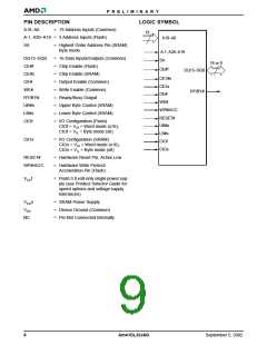
age. Standard control pins—chip enable (CE#f), write
enable (WE#), and output enable (OE#)—control nor-
mal read and write operations, and avoid bus
contention issues.
The devices requires only a single 3.0 volt power
supply for both read and write functions. Internally
generated and regulated voltages are provided for the
program and erase operations.
Simultaneous Read/Write Operations with
Zero Latency
The device offers complete compatibility with the
JEDEC single-power-supply Flash command set
standard. Commands are written to the command
register using standard microprocessor write timings.
Reading data out of the device is similar to reading
from other Flash or EPROM devices.
The Simultaneous Read/Write architecture provides
simultaneous operation by dividing the memory
space into two banks. The device can improve overall
system performance by allowing a host system to pro-
gram or erase in one bank, then immediately and
simultaneously read from the other bank, with zero la-
tency. This releases the system from waiting for the
completion of program or erase operations.
The host system can detect whether a program or
erase operation is complete by using the device sta-
tus bits: RY/BY# pin, DQ7 (Data# Polling) and
DQ6/DQ2 (toggle bits). After a program or erase cycle
has been completed, the device automatically returns
to reading array data.
The Am29DL32xG device family uses multiple bank
architectures to provide flexibility for different applica-
tions. Three devices are available with the following
bank sizes:
The sector erase architecture allows memory sec-
tors to be erased and reprogrammed without affecting
the data contents of other sectors. The device is fully
erased when shipped from the factory.
Device
DL322
DL323
DL324
Bank 1
Bank 2
28
4
8
24
Hardware data protection measures include a low
VCC detector that automatically inhibits write opera-
tions during power transitions. The hardware sector
protection feature disables both program and erase
operations in any combination of the sectors of mem-
ory. This can be achieved in-system or via
programming equipment.
16
16
The Secured Silicon (SecSi) Sector is an extra 256
byte sector capable of being permanently locked by
AMD or customers. The SecSi Sector Indicator Bit
(DQ7) is permanently set to a 1 if the part is factory
locked, and set to a 0 if customer lockable. This
way, customer lockable parts can never be used to re-
place a factory locked part.
The device offers two power-saving features. When
addresses have been stable for a specified amount of
time, the device enters the automatic sleep mode.
The system can also place the device into the
standby mode. Power consumption is greatly re-
duced in both modes.
Factory locked parts provide several options. The
SecSi Sector may store a secure, random 16 byte
ESN (Electronic Serial Number). Customer lockable
devices are one-time programmable and one-time
lockable.
2
Am41DL32x8G
September 5, 2002

 AMD [ AMD ]