P R E L I M I N A R Y
PIN DESCRIPTION
LOGIC SYMBOL
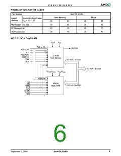
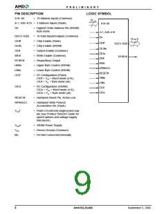
A18–A0
= 19 Address Inputs (Common)
19
A-1, A20–A19 = 3 Address Inputs (Flash)
A18–A0
SA
= Highest Order Address Pin (SRAM)
Byte mode
A-1, A20–A19
DQ15–DQ0
CE#f
= 16 Data Inputs/Outputs (Common)
= Chip Enable (Flash)
SA
16 or 8
CE#f
DQ15–DQ0
CE#s
= Chip Enable (SRAM)
CE1#s
CE2s
OE#
= Output Enable (Common)
= Write Enable (Common)
= Ready/Busy Output
WE#
RY/BY#
OE#
RY/BY#
UB#s
WE#
= Upper Byte Control (SRAM)
= Lower Byte Control (SRAM)
WP#/ACC
RESET#
UB#s
LB#s
CIOf
= I/O Configuration (Flash)
CIOf = VIH = Word mode (x16),
CIOf = VIL = Byte mode (x8)
LB#s
CIOs
= I/O Configuration (SRAM)
CIOs = VIH = Word mode (x16),
CIOs = VIL = Byte mode (x8)
CIOf
CIOs
RESET#
= Hardware Reset Pin, Active Low
WP#/ACC
= Hardware Write Protect/
Acceleration Pin (Flash)
V
CCf
= Flash 3.0 volt-only single power sup-
ply (see Product Selector Guide for
speed options and voltage supply
tolerances)
V
CCs
= SRAM Power Supply
VSS
NC
= Device Ground (Common)
= Pin Not Connected Internally
8
Am41DL32x8G
September 5, 2002

 AMD [ AMD ]