P R E L I M I N A R Y
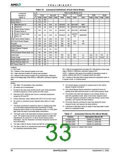
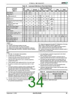
Table 18. Command Definitions (Flash Byte Mode)
Bus Cycles (Notes 2–5)
Command
Sequence
(Note 1)
First
Second
Third
Fourth
Fifth
Sixth
Addr Data Addr Data Addr Data Addr
Data
Addr Data Addr Data
Read (Note 6)
Reset (Note 7)
1
1
RA
RD
F0
XXX
(BA)
AAA
Manufacturer ID
4
6
4
4
AAA
AAA
AAA
AAA
AA
AA
AA
AA
555
555
555
555
55
55
55
55
90
90
90
90
(BA) 00
(BA) 02
01
(BA)
AAA
see
Table 19
Device ID
SecSi Sector Factory Protect
(Note 9)
(BA)
AAA
(BA)
X06
82/02
00
01
Sector Protect Verify
(Note 10)
(BA)
AAA
(SADD)
X04
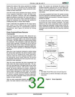
Enter SecSi Sector Region
Exit SecSi Sector Region
Program
3
4
4
3
2
2
6
6
1
1
1
AAA
AAA
AAA
AAA
XXX
XXX
AAA
AAA
BA
AA
AA
AA
AA
A0
90
555
555
555
555
PA
55
55
55
55
PD
00
55
55
AAA
AAA
AAA
AAA
88
90
A0
20
XXX
PA
00
PD
Unlock Bypass
Unlock Bypass Program (Note 11)
Unlock Bypass Reset (Note 12)
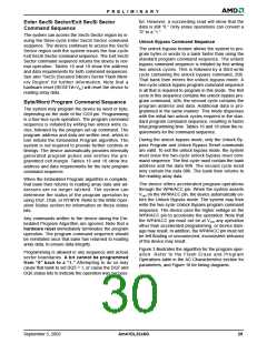
Chip Erase
XXX
555
555
AA
AA
B0
30
AAA
AAA
80
80
AAA
AAA
AA
AA
555
555
55
AAA
10
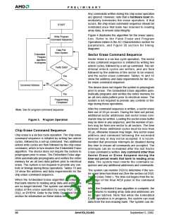
Sector Erase
55 SADD 30
Erase Suspend (Note 13)
Erase Resume (Note 14)
CFI Query (Note 15)
BA
55
98
Legend:
X = Don’t care
PD = Data to be programmed at location PA. Data latches on the rising
edge of WE# or CE#f pulse, whichever happens first.
RA = Address of the memory location to be read.
RD = Data read from location RA during read operation.
SADD = Address of the sector to be verified (in autoselect mode) or
erased. Address bits A20–A12 uniquely select any sector.
BA = Address of the bank that is being switched to autoselect mode, is
in bypass mode, or is being erased.
PA = Address of the memory location to be programmed. Addresses
latch on the falling edge of the WE# or CE#f pulse, whichever happens
later.
Notes:
1. See Table 1 for description of bus operations.
11. The Unlock Bypass command is required prior to the Unlock
Bypass Program command.
2. All values are in hexadecimal.
12. The Unlock Bypass Reset command is required to return to
reading array data when the bank is in the unlock bypass mode.
3. Except for the read cycle and the fourth cycle of the autoselect
command sequence, all bus cycles are write cycles.
13. The system may read and program in non-erasing sectors, or
enter the autoselect mode, when in the Erase Suspend mode.
The Erase Suspend command is valid only during a sector erase
operation, and requires the bank address.
4. Data bits DQ15–DQ8 are don’t care in command sequences,
except for RD and PD.
5. Unless otherwise noted, address bits A20–A12 are don’t cares.
6. No unlock or command cycles required when bank is in read
mode.
14. The Erase Resume command is valid only during the Erase
Suspend mode, and requires the bank address.
7. The Reset command is required to return to reading array data
(or to the erase-suspend-read mode if previously in Erase
Suspend) when a bank is in the autoselect mode, or if DQ5 goes
high (while the bank is providing status information).
15. Command is valid when device is ready to read array data or when
device is in autoselect mode.
8. The fourth cycle of the autoselect command sequence is a read
cycle. The system must provide the bank address to obtain the
manufacturer ID, device ID, or SecSi Sector factory protect
information. Data bits DQ15–DQ8 are don’t care. See the
Autoselect Command Sequence section for more information.
Table 19. Autoselect Device IDs (Byte Mode)
Device
Autoselect Device ID
55h (T), 56h (B)
Am29DL322G
Am29DL323G
Am29DL324G
50h (T), 53h (B)
9. The data is 80h for factory locked and 00h for not factory locked.
5Ch (T), 5Fh (B)
10. The data is 00h for an unprotected sector/sector block and 01h
for a protected sector/sector block.
T = Top Boot Sector, B = Bottom Boot Sector
September 5, 2002
Am41DL32x8G
33

 AMD [ AMD ]