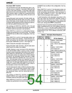
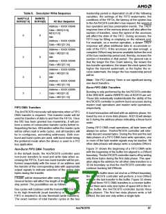
Table 9. Descriptor Write Sequence
mastership period is dependent on all of the following
variables: the settings of the FIFO watermarks, the
conditions of the FIFOs, the latency of the system bus
to the Am79C978 controller’s bus request, the speed of
bus operation and bus preemption events. The TRDY
response time of the memory device will also affect the
number of transfers, since the speed of the accesses
will affect the state of the FIFO. During accesses, the
FIFO may be filling or emptying on the network end.
For example, on a receive operation, a slower TRDY
response will allow additional data to accumulate in-
side of the FIFO. If the accesses are slow enough, a
complete DWord may become available before the end
of the bus mastership period and, thereby, increase the
number of transfers in that period. The general rule is
that the longer the Bus Grant latency, the slower the
bus transfer operations; the slower the clock speed, the
higher the transmit watermark; or the higher the re-
ceive watermark, the longer the bus mastership period
will be.
SWSTYLE
BWRITE
BCR20[7:0]
BCR18[5]
AD Bus Sequence
Address = XXXX XX04h
Data = MD2[15:0],
MD1[15:0]
0
X
X
Idle
Address = XXXX XX00h
Data = MD1[31:24]
Address = XXXX XX08h
Data = MD2[31:0]
Idle
2
Address = XXXX XX04h
Data = MD1[31:16]
Address = XXXX XX00h
Data = MD2[31:0]
Idle
3
3
0
1
Note: The PCI Latency Timer is not significant during
non-burst transfers.
Address = XXXX XX04h
Data = MD1[31:16]
Burst FIFO DMA Transfers
Address = XXXX XX00h
Data = MD2[31:0]
Bursting is only performed by the Am79C978 controller
if the BREADE and/or BWRITE bits of BCR18 are set.
These bits individually enable/disable the ability of the
Am79C978 controller to perform burst accesses during
master read operations and master write operations,
respectively.
Data = MD1[31:16]
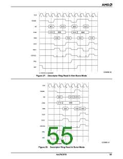
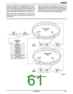
FIFO DMA Transfers
The Am79C978 microcode will determine when a FIFO
DMA transfer is required. This transfer mode will be
used for transfers of data to and from the FIFOs. Once
the BIU has been granted bus mastership, it will per-
form a series of consecutive transfer cycles before re-
linquishing the bus. All transfers within the master cycle
will be either read or write cycles, and all transfers will
be to contiguous, ascending addresses. Both non-
burst and burst cycles are used, with burst mode being
the preferred mode when the device is used in a PCI
bus application.
A burst transaction will start with an address phase, fol-
lowed by one or more data phases. AD[1:0] will always
be 0 during the address phase indicating a linear burst
order.
During FIFO DMA read operations, all byte lanes will
always be active. TheAm79C978 controller will inter-
nally discard unused bytes. During the first and the last
data phases of a FIFO DMA burst write operation, one
or more of the byte enable signals may be inactive. All
other data phases will always write a complete DWord.
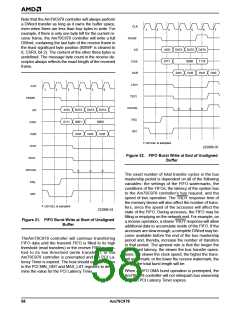
Figure 31 shows the beginning of a FIFO DMA write
with the beginning of the buffer not aligned to a DWord
boundary. TheAm79C978 controller starts off by writing
only three bytes during the first data phase. This oper-
ation aligns the address for all other data transfers to a
32-bit boundary so that the Am79C978 controller can
continue bursting full DWords.
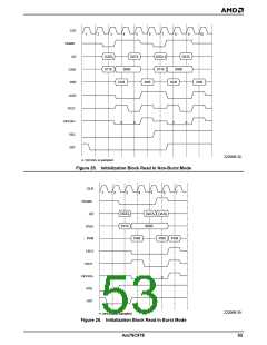
Non-Burst FIFO DMA Transfers
In the default mode, the Am79C978 controller uses
non-burst transfers to read and write data when ac-
cessing the FIFOs. Each non-burst transfer will be per-
formed sequentially with the issue of an address and
the transfer of the corresponding data with appropriate
output signals to indicate selection of the active data
bytes during the transfer.
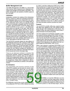
If a receive buffer does not end on a DWord boundary,
the Am79C978 controller will perform a non-DWord
write on the last transfer to the buffer. Figure 32 shows
the final three FIFO DMA transfers to a receive buffer.
Since there were only nine bytes of space left in the re-
ceive buffer, the Am79C978 controller bursts three
data phases. The first two data phases write a full
DWord, the last one only writes a single byte.
FRAME will be deasserted after every address phase.
Several factors will affect the length of the bus master-
ship period. The possibilities are as follows:
Bus cycles will continue until the transmit FIFO is filled
to its high threshold (read transfers) or the receive
FIFO is emptied to its low threshold (write transfers).
The exact number of total transfer cycles in the bus
Am79C978
57

 AMD [ AMD ]