AMD
P R E L I M I N A R Y
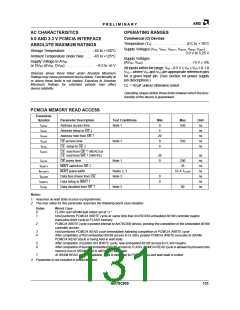
AC CHARACTERISTICS
OPERATING RANGES
Commercial (C) Devices
5.0 AND 3.3 V PCMCIA INTERFACE
Temperature (TA) . . . . . . . . . . . . . . . . . 0°C to + 70°C
ABSOLUTE MAXIMUM RATINGS
Supply Voltages (VCC, VDDT, VDDU1, VDDU2, VDDM, VDDP)
. . . . . . . . . . . . . . . . . . . . . . . . . . . . . . 3.0 V to 5.25 V
Storage Temperature: . . . . . . . . . . . . –65 to +150*C
Ambient Temperature Under Bias: . . . –65 to +125*C
Supply Voltages
(AVDD, VDD5) . . . . . . . . . . . . . . . . . . . . . . . . +5 V ± 5%
Supply Voltage to AVSS
or DVSS (AVDD, DVDD): . . . . . . . . . . . . . . –0.3 to +6 V
All inputs within the range: VSS – 0.5 V ≤ VIN ≤ VDD + 0.1 X
VDD – where VSS and VDD are appropriate reference pins
for a given input pin. (See section on power supply
pin descriptions.)
Stresses above those listed under Absolute Maximum
Ratings may cause permanent device failure. Functionality at
or above these limits is not implied. Exposure to Absolute
Maximum Ratings for extended periods may affect
device reliability.
CL = 50 pF unless otherwise noted
Operating ranges define those limits between which the func-
tionality of the device is guaranteed.
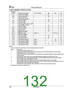
PCMCIA MEMORY READ ACCESS
Parameter
Symbol
tAVQV
tAVGL
Parameter Description
Address access time
Address setup to OE ↓
Address hold from OE ↑
CE access time
Test Conditions
Min
0
Max
Unit
ns
Note 1
550
5
ns
tGHAX
tELQV
20
0
ns
Note 1
550
ns
tELGL
CE setup to OE ↓
0
ns
tGHEH
CE hold from OE ↑ (READ) or
CE hold from WE ↑ (WRITE)
20
0
ns
ns
ns
ns
ns
ns
ns
tGLQV
tGLWTV
tWTLWTH
tGLQNZ
tQVWTH
tGHQZ
OE acess time
Note 1
200
35
WAIT valid from OE ↓
WAIT pulse width
Notes 2, 3
Note 3
53 X TCLKIN
Data Bus driven from OE
Data setup to WAIT ↑
Data disabled from OE ↑
0
0
Note 3
90
Notes:
1. Assumes no wait state access is programmed.
2. The max value for this parameter assumes the following worst case situation:
Value
Worst Case
0
1
FLASH and SRAM wait states set at “3.”
Host performs PCMCIA WRITE cycle at same time that Am79C930 embedded 80188 controller begins
instruction fetch cycle to FLASH memory.
2
PCMCIA WRITE cycle is posted internal to Am79C930 device, pending the completion of the embedded 80188
controller access.
3
4
Host performs PCMCIA READ cycle immediately following completion of PCMCIA WRITE cycle.
After completion of first embedded 80188 access to FLASH, posted PCMCIA WRITE executes to SRAM;
PCMCIA READ stycle is being held in wait state.
5
6
After completion of posted ISA WRITE cycle, new embedded 80188 access to FLASH begins.
After completion of second embedded 80188 access to FLASH, PCMCIA READ cycle is allowed to proceed onto
memory bus to SRAM; host is still held in wait state.
7
At SRAM READ cycle completion, data is delivered to PCMCIA bus and wait state is exited.
3. Parameter is not included in production test.
Am79C930
131

 AMD [ AMD ]