AMD
P R E L I M I N A R Y
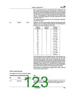
is set to a 0, the Baud Detect Count for Stop Diversity is not used in
the stop diversity decision logic.
1
0
UBDCS
URSSI
0
0
Use Baud Detect of Carrier Sense in CCA decision. When this bit is
set to a 1, the Baud Detect Count for Carrier Sense becomes one
input to the clear channel assessment logic. When this bit is set to a
0, the Baud Detect Count for Carrier Sense is not used in the clear
channel assessment decision.
Use RSSI in CCA and Stop Diversity decisions. When this bit is set
to a 1, the RSSI converted value comparison to the RSSI lower limit
becomes one input to the clear channel assessment logic and also
becomes one input to the Stop Diversity decision logic. When this
bit is set to a 0, the RSSI converted value comparison to the RSSI
lower limit is not used in the clear channel assessment logic and is
also not used in the Stop Diversity decision logic.
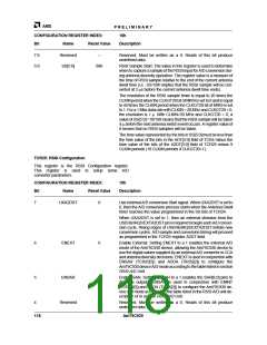
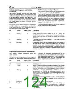
TCR29: Reserved
This register is a TAI reserved location.
CONFIGURATION REGISTER INDEX:
1Dh
Bit
Name
Reset Value
Description
7–0
Reserved
–
Reserved. Must be written as a 0. Reads of this bit produce
undefined data.
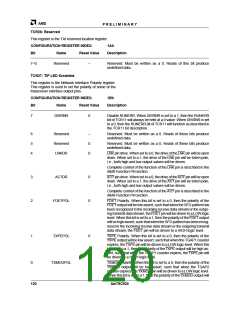
TCR30: Pin Function and Data Rate
This register is the Pin Function and Data Rate control
register. This register contains bits that control the
function of the ANTSLT, TXDATA, TXCMD, and TXC
pins as well as control bits to set the network data rate.
CONFIGURATION REGISTER INDEX:
1Eh
Bit
Name
Reset Value
Description
7
ANTSLTLFN
0
ANTSLT Function. ANTSLTLFN, ANTSLTLEN (TCR15[7]),
ANTSEN (TIR26[3]), and the PCMCIA pin are used to determine
the direction and data of the ANTSLT pin.
The control of the function of the ANTSLT/LA23 pin is described in
the Multi-Function Pin section.
6
TXDLFN
0
TXDATA Function. TXDLFN, TXDLEN (TCR15[6]), and the
PCMCIA pin are used to determine the direction and data of the
TXDATA pin.
The control of the function of the TXDATA/LA23 pin is described in
the Multi-Function Pin section.
5
4
TXCMFN
0
–
TXCMD Function. TXCMFN, TXCMEN (TCR15[5]), RCEN
(TIR11[3]), and the PCMCIA pin are used to determine the function
of the TXCMD pin.
USER7FN
Reserved. Must be written as 0. Reads of this produce
undefined data.
The control of the function of the TXCMD/LA21 pin is described in
the Multi-Function Pin section.
3
TXCIN
1
TXC Input. When set to a 0, the TXC pin functions as an output, pro-
viding a divide by X version of the CLKIN input, where X is deter-
mined by the setting of the DR bits of TCR30. When set to a 1, the
TXC pin functions as an input, allowing the data rate of the transmit
operations to be set by an external source. When TXCIN is set to 1,
122
Am79C930

 AMD [ AMD ]