AMD
P R E L I M I N A R Y
3–0
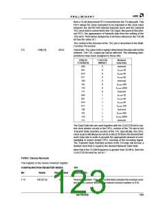
A2DT[3:0]
1010b
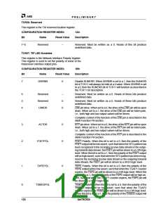
A/D sampling Time[3:0]. The value in the A2DT[3:0] field deter-
mines the duration of time required to convert the A/D input. Each
bit of resolution is equal to 4 times the CLKIN period when the
CLKGT20 bit of MIR9 is set to 0 and is equal to 8 times the CLKIN
period when the CLKGT20 bit of MIR9 is set to 1. For a 1Mbs data
rate with CLKIN = 20 MHz and CLKGT20 = 0, the resolution is 200
n. The A2DT value is used by all A/D modes, including the mode
that uses the internal A/D converter. The internal A/D converter
requires 600 nsec to convert – note that the default value of this reg-
ister is 2.0 µs for a CLKIN equal to 20MHz with the CLKGT20 bit set
to 0.
Note that the actual time for conversion is less than the A2DT pro-
grammed value by 1.5 CLKIN periods (with CLKGT20=0, it is 3
CLKINperiodsifCLKGT20=1). Thisfactisimportantwhenusingan
external A/D converter in the external A/D mode.
Minimum value in the A2DT[3:0] field must be 0001. A value of 0000
is not allowed.
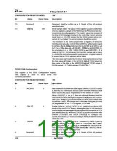
ADT[5:0]=TCR4[5:0]
ANTSLT
3 X tA
CCA_TEST
(Internal Signal)
SS[5:0]=TCR24[5:0]
START_A2D
(Internal Signal)
A2DT[3:0]=TCR25[3:0]+4 X tA
2 X tA
CACT=TIR27[7]
SAR[ 6:0]
When ENSAR = 1
tA
1 X tA
ADIN1
(when ENEXT=1)
6 X tA
6 X tA
3 X tA
3 X tA
ADIN2
(when ENEXT=1)
SAR_LATCH
(Internal Signal)
tA = period of CLKIN when CLKGT20 = 0
tA = (period of CLKIN) X 2 when CLKGT20 = 1
20138B-9
Note: ADIN1, ADIN2, and SAR_LATCH signals are only valid as shown when ENEXT (TCR25[6]) has been set to a 1.
Figure 3. Analog-to-Digital State Machine Timing
Am79C930
119

 AMD [ AMD ]