AMD
P R E L I M I N A R Y
then a 16-bit deep serial FIFO is inserted into the TX data path. This
FIFO allows for some mismatch to be tolerated in the clock rates
between the Am79C930 internal transmit clock and the external
TXC clock that is connected to the TXC input. Because of this inter-
nal FIFO, the appearance of transmit data from the setting of the
TXS bit in TIR8 will be delayed by 8 bit times whenever the TXCIN
bit has the value of 1.
The control of the function of the TXC pin is described in the Multi-
Function Pin section.
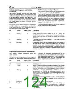
2:0
DR[2:0]
001b
Data Rate. The value in this register determines the data rate for the
network. The TXC output pin will be affected. The following inter-
pretations have been assigned to these bits:
DR[2:0]
TCR30[2:0]
CLKGT20
MIR9[7]
Network
Data Rate
000
001
010
011
100
101
110
111
000
001
010
011
100
101
110
111
0
0
0
0
0
0
0
0
1
1
1
1
1
1
1
1
reserved
fCLKIN÷20
fCLKIN÷40
fCLKIN÷80
reserved
fCLKIN÷200
fCLKIN÷2000
reserved
fCLKIN÷20
fCLKIN÷40
fCLKIN÷80
fCLKIN÷160
reserved
fCLKIN÷400
fCLKIN÷4000
reserved
The Data Rate bits are used together with the CLKGT20 bit to con-
trol clock divider circuits in the DPLL section of the TAI and in the
Transmit State machine section of the TAI. Specifically, the DPLL
clock source will always be set at a rate of 20 times the desired Net-
work Data rate in order to provide the appropriate amount of over-
sampling to insure proper DPLL tracking of the incoming signal.
The Transmit State machine section of the TAI logic will receive a
divided clock that is equal to the desired Network Data Rate.
Note that if the CLKIN frequency is greater than 20 MHz, then the
CLKGT20 bit must be set to 1.
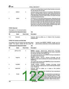
TCR31: Device Revision
This register is the Device Revision register.
CONFIGURATION REGISTER INDEX:
1Fh
Bit
Name
Reset Value
Description
7–0
REV[7:0]
01h
Revision Number. The value in this field contains the revision num-
ber for the current device. The lowest revision number is 01h.
Am79C930
123

 AMD [ AMD ]