AMD
P R E L I M I N A R Y
18h
CONFIGURATION REGISTER INDEX:
Bit
Name
Reset Value
Description
7:6
5:0
Reserved
SS[5:0]
–
Reserved. Must be written as a 0. Reads of this bit produce
undefined data.
00h
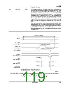
RSSI Sample Start. The value in this register is used to determine
when to capture a sample of the RSSI input for A/D conversion dur-
ing antenna diversity operation. The register value is a measure of
the time of RSSI sample relative to the end of the current antenna
dwell time (i.e., SS=03h implies that the RSSI sample will be con-
verted at 3 µs before the current antenna dwell time ends).
The resolution of the RSSI sample timer is equal to 20 times the
CLKIN period when the CLKGT20 bit of MIR9 is set to 0 and is equal
to 40 times the CLKIN period when the CLKGT20 bit of MIR9 is set
to 1. For a 1 Mbs data rate with CLKIN = 20 MHz and CLKGT20 = 0,
the resolution is 1 µ. With CLKIN=20 MHz and CLKGT20 = 0, a
value of SS[5:0] = 00100 means that the RSSI sample will be taken
4 µ before the next antenna switch event occurs. A register value of
0 means that no RSSI samples will be taken.
The time value represented by the bits in SS[5:0] must be less than
the time value of the bits in the ADT[5:0] field of TCR4 minus the
time value of the bits of the A2DT[3:0] field of TCR25 minus 9
CLKIN periods (18 CLKIN periods if CLKGT20=1).
TCR25: RSSI Configuration
This register is the RSSI Configuration register.
This register is used to setup some A/D
converter parameters.
CONFIGURATION REGISTER INDEX:
19h
Bit
Name
Reset Value
Description
7
UXA2DST
0
Use external A/D conversion Start signal. When UXA2DST is set to
0, then the A/D conversion process starts when the Antenna Dwell
timer reaches the value programmed in the SS bits of TCR24.
When UXA2DST is set to 1, then an external stimulus from the
USER6/IRQ5/EXTA2DSTpinisrequiredtobegineachA/Dconver-
sion cycle. Rising edges of USER6/IRQ5/EXTA2DST initiate new
conversion cycles. A/D sample and conversion timing will proceed
as programmed in the TCR25 register A2DT field.
6
5
ENEXT
0
Enable External. Setting ENEXT to a 1 enables the external A/D
mode of the Am79C930 device, allowing the Am79C930 device to
use the digital values supplied by an external A/D converter in CCA
and antenna diversity decisions. ENEXT is used in conjunction with
ENSAR (TCR25[5]) and ADDA (TIR26[2]) to configure the
Am79C930 device A/D mode according to the table listed in section
RSSI A/D Unit.
ENSAR
0
–
Enable SAR. Setting ENSAR to a 1 enables the SAR[6:0] pins to
drive as outputs. ENSAR is used in conjunction with ENINT
(TCR25[6]) and ADDA (TIR26[2]) to configure the Am79C930 de-
vice A/D mode according to the table listed in the RSSI A/D unit de-
scription of in section RSSI A/D Unit.
4
Reserved
Reserved. Must be written as a 0. Reads of this bit produce
undefined data.
118
Am79C930

 AMD [ AMD ]