AMD
P R E L I M I N A R Y
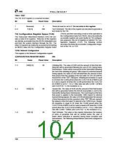
TIR31: TEST
The TAI TEST register is a reserved location.
Bit
Name
Reset Value
Description
7
Reserved
TC[6:0]
0
These bit must be set to 0. Do not write to this register.
6–0
00h
Test Command. The bits in this register are decoded to generate a
test mode for the TAI.
(TIR24) and then executing a read or write operation to
TAI Configuration Register Space (TCR)
the Configuration Data Port (TIR25). Since the indirectly
accessible registers are used mostly for TAI configura-
tion purposes, this set of registers is labeled TAI Con-
figuration Registers (TCR). The following section
describes the indirectly accessible Configuration Regis-
ters of the TAI, or TCR.
The Transceiver Attachment Interface (TAI) Unit con-
tains a total of 64 registers. Thirty-two of the registers
are directly accessible from the 80188 embedded core
and from the system interface through the BIU. The
other 32 registers are indirectly accessed by first writing
an INDEX value into the Configuration Register Index
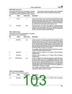
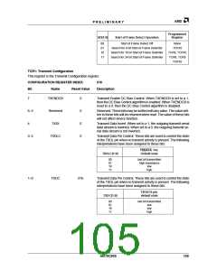
TCR0: Network Configuration
This register is the Network Configuration register.
CONFIGURATION REGISTER INDEX:
00h
Bit
Name
Reset Value
Description
7–5
DRB[2:0]
0h
Dribbling Bits. The value of DRB sets the amount of time that drib-
bling bits will be generated following the end of CRC during frame
transmission. Power will be removed from the transmitter following
the end of the dribbling bit period. With respect to external transmit
timing signals, the value of DRB will determine the amount of time
that passes from the sending of the last valid TX CRC bit until the
deassertion of the TXP_ONsignal. Dribbling bit resolution is equal
to 40 times the CLKIN period when the CLKGT20 bit of MIR9 is set
to 0 and is equal to 80 times the CLKIN period when the CLKGT20
bit of MIR9 is set to 1. For a 1 Mbs data rate with CLKIN = 20 MHz
and CLKGT20 = 0, the resolution is 2 µ.
4–2
HDB[2:0]
0h
Header Bits. The value of HDB sets the amount of time that header
bits will be generated before the first bit of preamble is sent to the
transmitter during frame transmission. The count begins at the time
that power is applied to the transmitter. With respect to external
transmit timing signals, the value of HDB will determine the amount
of time that passes from the assertion of the TXP_ON and signal to
the delivery of the first valid TX data bit to the TXDATA pin. Header
bit resolution is equal to 40 times the CLKIN period when the
CLKGT20 bit of MIR9 is set to 0 and is equal to 80 times the CLKIN
period when the CLKGT20 bit of MIR9 is set to 1. For a 1 Mbs data
rate with CLKIN = 20MHz and CLKGT20 = 0, the resolution is 2 µ.
1–0
SD[1:0]
0h
Start Delimiter. The value in this register determines the number
of bytes of preamble that will be verified before the start of
frame detect indication is asserted during frame reception and
transmission. The following interpretations have been assigned to
these bits.
104
Am79C930

 AMD [ AMD ]