AMD
P R E L I M I N A R Y
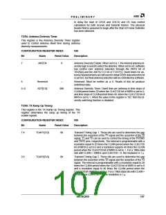
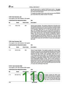
TCR6: TX Ramp Down Timing
This register is the TX Ramp Down Timing register.
This register determines the ramp down timing of the TX
enable signals.
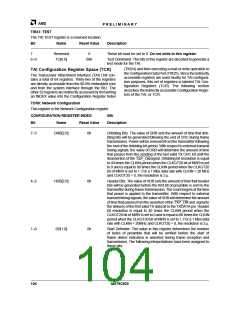
CONFIGURATION REGISTER INDEX:
06h
Bit
Name
Reset Value
Description
7:4
TGAP3[3:0]
0h
Transmit Timing Gap 3. These bits are used to determine the gap
between the deassertion of theT3 signal and the deassertion of the
T2 signal. T3 and T2 can be used to control the timing of the
TXMOD and TXPE pins. The interval is programmable with a reso-
lution equal to 20 times the CLKIN period when the CLKGT20 bit of
MIR9 is set to 0 and a resolution equal to 40 times the CLKIN period
when the CLKGT20 bit of MIR9 is set to 1. For a 1 Mbs data rate with
CLKIN = 20 MHz and CLKGT20 = 0, the resolution is 1 µ.
3:0
TGAP4[3:0]
0h
Transmit Timing Gap 4. These bits are used to determine the gap
between the deassertion of theT2 signal and the deassertion of the
T1 signal. T2 and T1 can be used to control the timing of the TXPE
and TXCMD pins. The interval is programmable with a resolution
equal to 20 times the CLKIN period when the CLKGT20 bit of MIR9
is set to 0 and a resolution equal to 40 times the CLKIN period when
the CLKGT20 bit of MIR9 is set to 1. For a 1Mbs data rate with
CLKIN = 20 MHz and CLKGT20 = 0, the resolution is 1 µ.
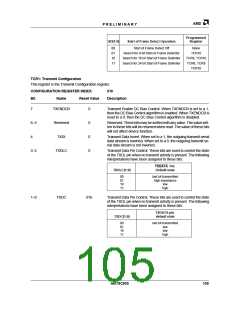
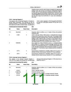
TCR7: Pin Data A
This register is the Pin Data A register. This register is
TXDATA and TXCMD pins and to configure the function
used to deliver and retrieve data from the ANTSLT,
of the USER5 and USER6 pins.
CONFIGURATION REGISTER INDEX:
07h
Bit
Name
Reset Value
Description
7
CTSEN
0
CTS Enable. When CTSEN is set to a 1, then the USER1/IRQ12 pin
input value will be used to gate the start of the internal TX state ma-
chine. With CTSEN set to a 1, T1, T2, etc., signaling will not follow
the assertion of the TXS bit of TIR8 until USER1/IRQ12/EXTCTS
becomes active (HIGH), and then normal timing forT1, T2, etc., will
be produced.
When CTSEN is set to a 0, then TX state machine operations pro-
ceed without delay, following the assertion the TXS bit of TIR8, re-
gardless of the value of USER1/IRQ12/EXTCTS.
6
USER6FN
0
USER6 Function. USER6FN, the PCMCIA mode pin, USER6EN
(TCR15[3]), and the ISA Plug and Play registers 70h and 71h are
used to determine the function of the USER6/IRQ5 pin.
In addition, the USER6/IRQ5 pin may be used to produce interrupts
to the 80188 embedded controller. This capability is controlled by
the ENXSDF bit of TCR28 and the SDFU bit of TIR5 and operates
independently of the bits mentioned above.
The control of the function of the USER6/IRQ5 pin is described in
the Multi-Function Pin section.
5
USER5FN
0
USER5 Function. USER5FN, the PCMCIA mode pin, USER5EN
(TCR15[2]), and ISA PnP registers 70h and 71h are used to deter-
mine the function of the USER5/IRQ4 pin.
108
Am79C930

 AMD [ AMD ]