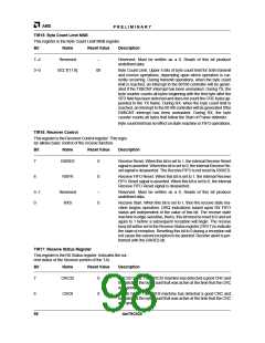
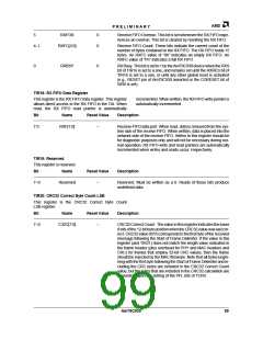
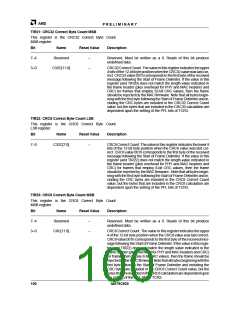
AMD
P R E L I M I N A R Y
2
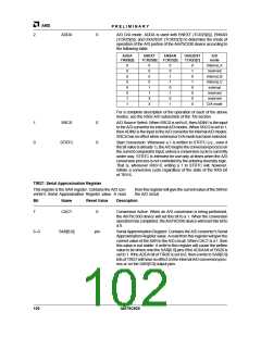
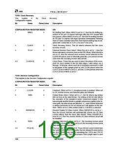
ADDA
0
A/D D/A mode. ADDA is used with ENEXT (TCR25[6]), ENSAR
(TCR25[5]), and UXA2DST (TCR25[7]) to determine the mode of
operation of the A/D portion of the Am79C930 device according to
the following table:
ADDA
TIR26[2]
ENEXT
TCR25[6]
ENSAR
TCR25[5]
UXA2DST
TCR25[7]
A/D
mode
0
0
0
0
0
0
1
1
0
0
0
0
1
1
X
X
0
0
1
1
0
1
0
1
0
1
internal_A
reserved
internal_B
internal_C
external
0
1
X
X
X
X
reserved
reserved
D/A mode
For a complete description of the operation of each of the above
modes, see the RSSI A/D subsection of the TAI section.
1
0
SRCS
0
0
A/D Source Select. When SRCS is set to 0, then ADIN1 is the input
to the A/D converter for internal A/D modes. When SRCS is set to 1,
then ADIN2 is the input to the A/D converter for internal A/D modes.
SRCS has no effect when external or D/A mode has been selected.
STRTC
Start Conversion. Whenever a 1 is written to STRTC (i.e., even if
the bit value is already 1), the A/D begins the conversion process on
the current comparator input, unless a conversion cycle is currently
under way. STRTC is intended for use only at times when the A/D
conversion process is not controlled by the antenna diversity logic.
That is, whenever RXS=0, writing a 1 to STRTC will; however,
initiate a conversion cycle regardless of the state of the RXS bit
of TIR16.
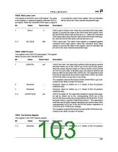
TIR27: Serial Approximation Register
This register is the SAR register. Contains the A/D con-
verter’s Serial Approximation Register value. A read
from this register will give the current value of the SAR in
the A/D circuit.
Bit
Name
Reset Value
Description
7
CACT
0
Conversion Active. When an A/D conversion is being performed,
the Am79C930 device will set this bit to a 1. When the conversion
operation has completed, the Am79C930 device will reset this bit to
a 0.
6–0
SAR[6:0]
pin
Serial Approximation Register. Contains the A/D converter’s Serial
Approximation Register value. A read from this register will give the
current value of the SAR in the A/D circuit. When CACT is a 1, then
this value is not stable. A write to this register will cause the written
value to be driven onto the SAR[6:0] pins if the ADDA bit of TIR26 is
set to 1. If the ADDA bit of TIR26 is set to 0, then a write to SAR[6:0]
bits of TIR27 will have no effect on the internal A/D conversion proc-
ess or on the SAR[6:0] output pins.
102
Am79C930

 AMD [ AMD ]